Introduction
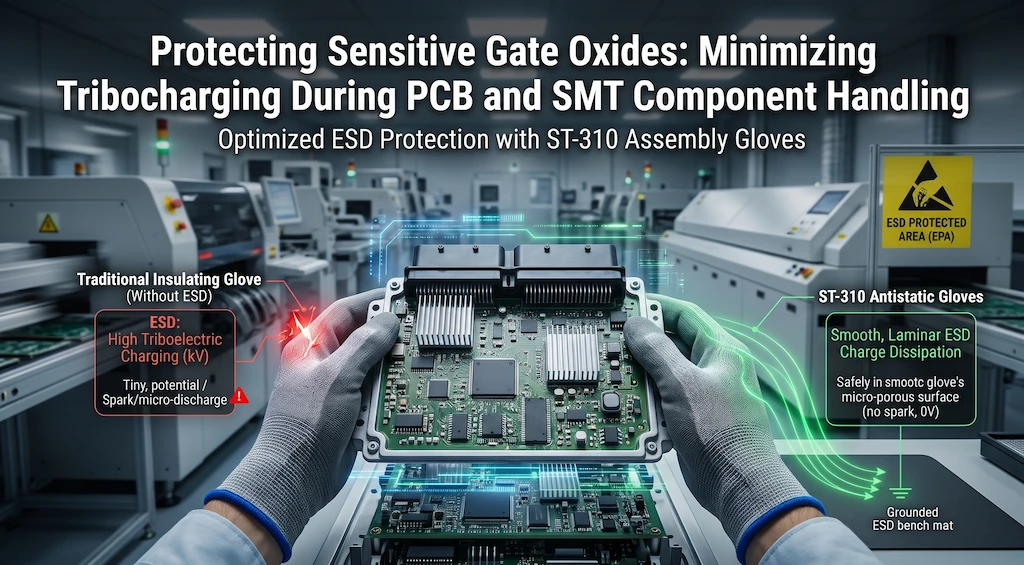
In the manufacturing of electronic control units (ECUs) for new energy vehicles, battery management systems (BMS), and megawatt-class high-voltage industrial variable-frequency drives, “zero defects” and long-term operational reliability are the fundamental principles of production line quality control. As the manufacturing processes for automotive-grade power semiconductors and main control chips continue to shrink, the gate insulation layer thickness of power MOSFETs, IGBT driver chips, and highly integrated MCUs has been reduced to the nanometer-level limit. On these high-density mixed-assembly production lines, what truly causes a collapse in batch quality is often not direct burnout caused by violent discharges of several thousand volts, but rather low-potential electrostatic discharges generated by tribocharging—the accumulation of static electricity due to slight friction—when operators handle materials at high speeds. This micro-stress charge can cause hidden lattice damage within the chip, allowing the board to narrowly pass factory functional testing but leading to sudden, premature breakdown under the harsh operating conditions of a vehicle.
To completely break the chain of charge accumulation at high-frequency friction workstations—such as PCB handling, post-reflow inspection, and enclosure assembly—the engineering team must redefine protection standards at the physical contact interface and comprehensively implement automotive-grade PCB assembly antistatic work gloves. Relying on a continuous, homogeneous topological structure of conductive fibers, these gloves smoothly divert transient charges generated by separation friction between the operator’s body and the edges of the circuit board into a ground loop, thereby preventing any localized high-potential spark discharges. When establishing a systematic human-machine protection network covering the entire Electrostatic Protection Area (EPA), proper selection is critical for meeting the requirements of different humidity conditions and workstation cleanliness levels. To systematically review the full range of protective solutions covering various substrate densities, coating types, and surface impedance gradients, please refer to the ESD Safe & Antistatic Gloves main category overview, which includes a wide variety of specialized protective equipment for electronics manufacturing.
Physics of Latent Gate Oxide Breakdown: The Hidden Threat to Automotive Electronics
In automotive electronic control units and new energy vehicle power management systems, highly integrated microcontrollers (MCUs), driver ICs, and power MOSFETs are central to performing logic calculations and high-current inversion. While these semiconductor devices achieve microsecond-level switching response, the physical breakdown voltage limits of their internal insulation structures have been compressed into an extremely narrow window. The vast majority of chip damage caused by electrostatic discharge (ESD) does not result from macroscopically visible, violent arc burn-through, but rather from dielectric degradation occurring at the atomic level; this latent structural defect is the underlying root cause of the intractable early-life failure rate in automotive electronics after they leave the factory.
Nanometer SiO₂ Dielectric Limits and the 50V Arc Vulnerability
In the gate structures of modern advanced-process logic chips and power MOSFETs, the silicon dioxide (SiO₂) dielectric layer serves as a critical barrier that physically isolates and controls the gate from the conductive channel:
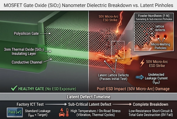
Nanometer-scale dielectric layers and extremely high electric field strength thresholds: With the widespread adoption of deep submicron processes and compact trench-gate architectures, the physical thickness of the gate SiO₂ layer has generally been reduced to the range of 2 to 5 nanometers. Although the theoretical intrinsic breakdown field strength of SiO₂ grown via high-purity thermal oxidation can reach 10 MV/cm, at the absolute microscopic scale of a few nanometers, its absolute breakdown voltage threshold has been compressed to a safe limit range of approximately 10 V to 20 V;
50-V Micro-Arcs and Latent Breakdown Mechanisms: During the handling of circuit boards in the workshop and at assembly stations, micro-discharge arcs as low as 50 V can easily occur when a person comes into contact with the exposed leads of a chip via the edge of a workpiece. The energy released by this low-voltage discharge is extremely small, insufficient to instantly destroy the external bonding wires or break down the protective diodes; but the resulting transient microelectric field is sufficient to exceed the dielectric strength of the SiO₂ film, triggering a surge in Fowler-Nordheim tunneling current within it, thereby causing localized microscopic traps and dielectric pinholes in the crystal lattice;
The Fatal Logic of Evading ICT/FCT Testing on the Production Line: A MOSFET subjected to 50V microstress damage—even though its gate oxide layer has been compromised—typically exhibits a weak gate leakage current (I_gss) that remains within the tolerance range specified in the datasheet during room-temperature factory testing (including In-Circuit Testing (ICT) and Functional Testing (FCT)), and the functional logic still classifies it as “Pass.” However, once the vehicle is delivered and put into service, when exposed to high temperatures of up to 125 degrees Celsius in the engine compartment, high vibration stress, and frequent reverse spike surges from inductive loads, localized thermal stress at the damaged micro-pores rapidly accelerates electromigration. This ultimately triggers a sudden, complete gate breakdown and short circuit, causing the vehicle’s ECU to suddenly lose control while driving.
Human Body Model (HBM) and Triboelectric Generation Mechanisms
To understand the process by which electrostatic hazards in the workshop are amplified, it is essential to reverse-engineer the mechanisms based on the ANSI/ESDA/JEDEC JS-001 Human Body Model (HBM), which is commonly used in semiconductor reliability engineering:
Equivalent Physical Circuit for Human Body Charge Storage: In electrostatic protection theory, a human body without grounding protection can be modeled as a lumped-parameter circuit—with an equivalent capacitance (C) of approximately 100 picofarads (pF) and an equivalent series resistance (R) of approximately 1,500 ohms. The human skin is isolated from the antistatic epoxy flooring by the insulating medium of the shoe sole, forming a natural, high-capacitance charge collection reservoir;
Low-energy micro-movements trigger kilovolt-level high-potential accumulation: When an assembly line worker stands up from an insulated chair, walks with the rubber soles of their shoes experiencing slight friction against the floor, or quickly raises their forearm, according to the principle of charge conservation (Q = C × V), microscopic charge transfer at the contact-separation interface causes the body’s total capacitance to drop sharply the moment it leaves the ground, causing the body’s electrostatic potential to surge from tens of volts to highly dangerous levels of 2,000 V or even over 5,000 V within a few seconds;
Nanosecond-scale transient pulse energy injection: When an operator carrying a static charge of several thousand volts directly grips the edge of a PCBA board with bare hands or while wearing insulated gloves, the nano-coulomb (nC) level of static charge stored within the body will discharge through the chip pins to the ground reference layer via a damped oscillatory discharge with a rise time of less than 10 nanoseconds (ns). The peak discharge current can often reach several amperes. When this transient energy penetrates the protective network and reaches the chip’s sensitive gate oxide layer, it is sufficient to generate localized hotspots on the microscopic nanosecond scale, directly destroying micron-scale core circuit elements.
Triboelectric Mechanics at the Workstation: FR-4 Substrates & Polymeric Trays
At surface-mount technology (SMT) and automotive ECU assembly workstations, circuit boards are not always stationary. When operators perform component insertion, workpiece transfer, functional test fixture clamping, and housing assembly, their hands repeatedly contact and pick up printed circuit boards (PCBs) at a rate of several dozen times per minute. This continuous, rapid handling constitutes a typical contact-separation charging process at the interface between the polymer and the solder mask; even minor mismatches in the triboelectric properties of any materials at the workstation can create a sustained charge pumping effect between the operator’s fingertips and the edges of the substrate.
Contact-Separation Charging on Epoxy-Glass PCB Edges
Automotive-grade PCBA substrates are primarily made of FR-4 epoxy-glass fiber laminates and are extensively coated with a photosensitive solder mask:
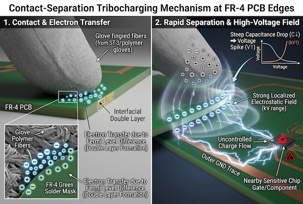
Contact potential difference and electron transfer at polymer interfaces: FR-4 resin and common thermosetting solder mask inks are strongly negatively polar materials that readily accept electrons in the triboelectric series, whereas ordinary polyester fibers or traditional insulating nitrile rubber layers are relatively more positively polar. When a finger wearing a conventional glove grips the edge of a PCB, the contact surface of the glove interlocks tightly with the microscopically rough surface of the solder mask. The difference in Fermi levels at the interface forces electrons to instantaneously jump unidirectionally from the molecular chains of the glove to the surface of the ink, forming a microscopic double layer;
Sudden Potential Spike Caused by High-Speed Physical Separation: When the finger releases or rapidly moves away from the edge of the circuit board, mechanical separation occurs instantaneously at the contact surface. As the separation distance expands from micrometers to macroscopic distances within microseconds, the equivalent capacitance between the two decreases sharply; according to the principle of charge conservation, the net free negative charge remaining on the solder mask layer and the glass fiber fracture surface causes the potential at the PCB edge to surge to hundreds or even thousands of volts within a few milliseconds;
Localized Discharge Triggered by the Potential Difference on the Board: This static charge accumulated at the edge of the FR-4 cannot be rapidly dissipated through the epoxy substrate itself; the moment the circuit board is inserted into a test fixture or comes into contact with the positioning pins of a metal chassis, the accumulated uncontrolled potential directly generates a strong, localized high-frequency displacement current through the outer ground copper trace (GND Trace). This current travels along the return path into nearby filter capacitors and driver ICs, constituting the physical source of early dielectric insulation degradation.
Electrostatic Transfer Dynamics in SMT Reel-to-Board Operations
In addition to edge gripping of the circuit boards themselves, material replenishment around the SMT placement machine and the handling of semi-finished product trays are another major scenario prone to electrostatic discharge:
Mechanisms of induced charging during high-speed tape peeling: During high-speed feeder feeding and tape-to-board transfer operations in SMT, operators must rapidly peel off the transparent cover tape from the plastic carrier tape. The friction generated by peeling the polymer cover tape often induces a strong electrostatic field of several thousand volts on the tape itself; if the operator’s hands do not form a continuous, low-impedance discharge path, this strong electrostatic field will induce oppositely polarized charges on the leads of micro SMT components placed in the tape grooves, resulting in a Field-Induced CDM (Charge-Dissipative Model);
High-frequency transfer paths at the interface of anti-static blister trays: Anti-static blister trays used to hold bare automotive ECU boards or power MOSFET modules typically rely solely on a trace amount of surfactant coating to achieve anti-static properties. In low-humidity workshop environments or after frequent friction and wear, the inner walls of the trays are prone to degrading into a state of localized high-resistance insulation; when an operator quickly pulls a PCBA board vertically out of a tray slot, the friction and separation between the inner wall of the slot and the dense pins on the board’s underside can also generate significant charge transfer;
Micro-spark hard breakdown at the moment of pin contact: During the extremely brief instant when a device pin carrying induced charge moves with the board and comes into contact with a grounded metal carrier, an automated dispensing needle, or a test probe, the air gap breaks down, accompanied by the release of an ultra-fast pulse current on the order of nanoseconds. This CDM-mode discharge is characterized by an extremely short discharge duration and an extremely high peak current. Its energy is concentrated in the extremely small ohmic contact area and the gate edge within the chip, making it highly likely to permanently destroy the ESD diodes and gate insulation layers of the chip’s core pins without leaving any visible external physical burn marks.
Charge Neutralization Architecture: The ST-310 Engineered Dissipation Path
In automotive-grade SMT manufacturing and industrial control board assembly workstations, relying solely on insulation or haphazard grounding often fails to resolve charge transfer issues. The core engineering logic of electrostatic protection lies in controlling the rate and path of charge neutralization, ensuring that charges generated by friction neither remain on the interface for extended periods—forming high-voltage electric fields—nor result in sudden hard discharges in the form of nanosecond-scale transient pulses. The ST-310 establishes a controlled, homogeneous charge dissipation path through the microscopic topological weaving of its inner lining and impedance engineering of its palm-side coating.
Seamless Carbon-Grid Matrix and Resistivity Control (1.0×10⁶ to 1.0×10⁸ Ohms)
The arrangement of conductive fibers within the glove liner directly determines the continuity and isotropy of the charge dissipation pathways:
13-gauge seamless carbon fiber 3D mesh: The ST-310 features a seamless composite weave (13-gauge seamless carbon/polyester liner) of continuous filament polyester at a density of 13 gauges and highly conductive bicomponent carbon fibers. During the circular knitting process, the conductive carbon fibers are woven into a mesh at microscopic, uniform intervals of approximately 5 mm in both the warp and weft directions, eliminating the “conductive dead zones” caused by fiber breaks or knots found in traditional coarse textiles;
The Physical Balance Logic of the Optimal Dissipative Range: According to the ANSI/ESD S20.20 standard, the point-to-point resistance (Rp-p) of anti-static work gloves must be strictly controlled within the dissipative range of 1.0×10⁶ to 1.0×10⁸ ohms:
The anti-accumulation threshold at the upper limit of 1.0×10⁸ ohms: If the surface resistivity exceeds 1.0×10⁹ ohms, the material exhibits insulating properties and cannot dissipate triboelectric charges within process cycles ranging from nanoseconds to microseconds, resulting in the continuous accumulation of high voltages—up to several thousand volts—at the fingertips;
Lower limit: 1.0×10⁶ ohm surge protection threshold: If the surface resistance is too low (falling below 1.0×10⁵ ohms into the conductive range), contact between charged components and the glove will trigger a violent “hard grounding” micro-spark discharge within a few nanoseconds, which can easily cause thermal breakdown of the gate insulation under the Charged Device Model (CDM);
Impedance Stability in Low-Humidity Conditions: The ST-310’s homogeneous carbon mesh relies directly on conductive molecular chains to transfer charge, without depending on moisture-absorbing surfactants in the air. Even in extremely dry workshops where relative humidity falls below 25% RH during winter, the impedance remains locked within the specified range, eliminating impedance drift and protection failure caused by environmental fluctuations.
Controlled Palm-Coated Grounding Loop via ESD Bench Mats
During the actual handling and transfer of PCBA boards, the coating structure of the gloves directly influences the effective charge dissipation path between the operator and the ESD bench mat:
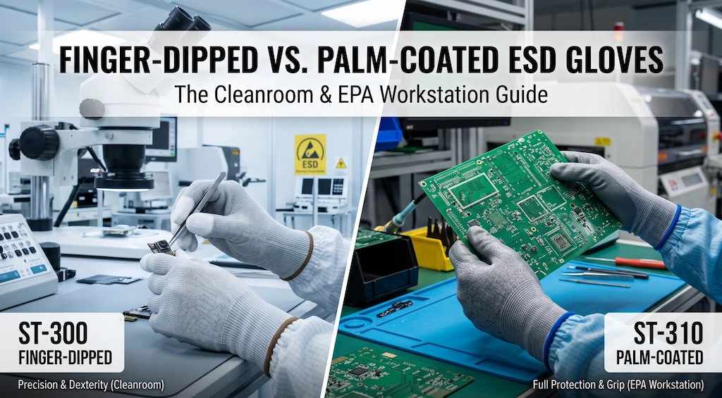
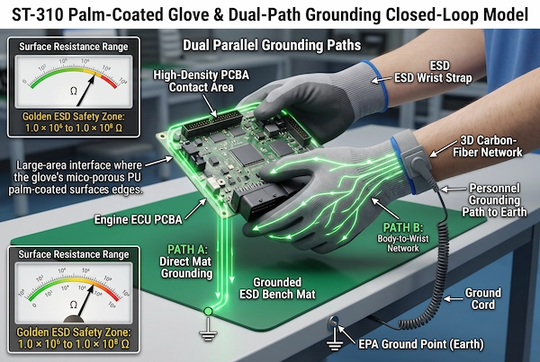
The advantage of doubled geometric contact area with full-palm coating: Compared to finger-coated gloves that cover only a 2- to 3-centimeter area at the fingertips, the ST-310 employs a polyurethane coating process (Palm-Coated) that fully covers the palm and fingertips. When an operator supports the edges of a large automotive ECU or industrial control inverter motherboard with both hands, the extensive conductive microporous rubber layer on the palms and inner sides of the knuckles establishes a sufficient physical contact surface with the board’s peripheral grounding pads, bezels, and the edges of the ESD bench mat, expanding the geometric discharge contact area several times over and thereby significantly reducing contact interface resistance;
Dual-Path Smooth Discharge Closed-Loop Grounding: When an operator’s hand comes into contact with an FR-4 board carrying triboelectric charge, the charge is no longer confined to a single fingertip for point discharge. Instead, it is rapidly homogenized and dispersed through the ST-310’s microporous network on the palm. One path directs the charge to ground via the operator’s wrist strap and conductive rubber shoes, while simultaneously forming a low-inductance parallel shunt discharge circuit the moment the palm contacts the grounded anti-static workpad, smoothly extending the discharge duration to the microsecond range and effectively dissipating transient voltage pulses;
Criteria for coating selection based on workstation characteristics: Between micro SMT placement, handling of lightweight optical lenses, and handling of heavy-duty automotive-grade PCBA, finger-dipped and palm-dipped processes exhibit distinctly different engineering characteristics in terms of charge dissipation area and mechanical anti-slip torque. For an in-depth evaluation of the technical differences between the two coating processes in terms of cleanroom class compatibility and workstation flow resistance, please refer to the specialized comparative analysis, Finger-Dipped vs. Palm-Coated ESD Gloves.
Chemical Purity and Mechanical Grip in High-Density SMT Workstations
In automotive-grade SMT placement and board-level assembly lines, gloves serve not only as a means of dissipating electrostatic charges but also as physical tools that come into direct contact with exposed copper pads, the terminals of micro-components, and the interfaces of IPX/IPY/IPZ coatings. Throughout their entire lifecycle, automotive electronics and industrial control boards are subjected to multiple harsh stresses, including high temperatures, high humidity, sulfuric corrosion, and continuous mechanical vibration. The chemical inertness and surface friction properties of glove coatings directly determine the microstructural metallurgical reliability of solder joints and the safety of handling large-size PCBA boards.
Zero Ionic Contamination and Solderability Preservation
Automotive electronics adhere to extremely stringent ionic cleanliness control standards (such as IPC-J-STD-001 and IPC-5704) to prevent interface degradation caused by chemical migration:
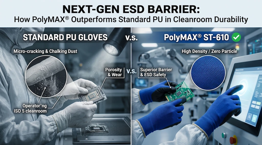
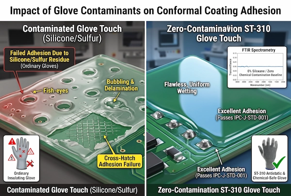
Strict control over sulfur-free and silicone-free formulations: Traditional low-end personal protective equipment (PPE) or standard anti-static gloves often use sulfur-containing cross-linking agents during the vulcanization dipping process, or incorporate silicone-based release agents and defoamers. Free sulfides react in situ with the bare copper pads or electroless gold (ENIG) layer on the PCBA, forming an insulating copper sulfide (Cu₂S) film; Meanwhile, free silicone oil molecules readily migrate to the pad surface, forming a low-surface-energy, hydrophobic barrier layer that is difficult to clean. During subsequent reflow soldering, this layer hinders flux activation, leading to widespread de-wetting, micro-voids, and solder ball splatter;
Eliminates the Leaching and Migration of Halogens and Reactive Ions: ST-310 employs a high-purity water-based cleaning process and a sulfur-free formulation. Ion chromatography (IC) testing strictly controls the content of easily ionized, corrosive ions such as chloride (Cl⁻), sodium (Na⁺), and potassium (K⁺); Prevents the release of conductive salt mist particles when operators handle board edges or exposed vias, eliminating at the source the chemical risks of dendritic growth and micron-level short circuits and leakage in humid, powered environments;
Ensures adhesion at the conformal coating interface: After soldering is completed on automotive ECU and new energy BMS circuit boards, the entire board must be sprayed with an acrylic, polyurethane, or silicone-based conformal coating to isolate moisture and salt fog. If chemical plasticizers or release agents remain on the surface of the work gloves, they can contaminate the board surface, causing localized imbalances in surface tension in the coating. After spraying and curing, this can result in mottling, bubbles, fish-eyes, and failure in the cross-cut adhesion test, thereby compromising the overall environmental protection rating. The chemically inert coating of the ST-310 leaves no fingerprints or chemical residues upon contact, ensuring a dense bond between the conformal coating film and the epoxy-glass fiber board substrate.
Anti-Slip Ergonomics for Handling Heavy Automotive PCBA Boards
PCBA boards for automotive center-console displays, high-voltage on-board chargers (OBCs), and chassis control systems typically incorporate large-area, thick-copper heat sinks, large electrolytic capacitors, magnetic inductors, and die-cast aluminum alloy brackets, with total weights often ranging from several hundred grams to several kilograms:
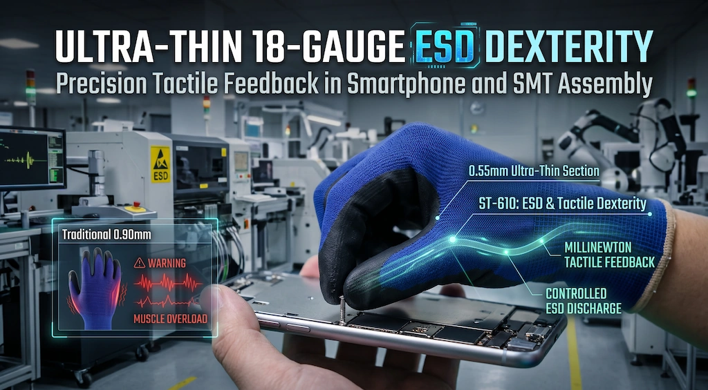
Friction Mechanics of Microporous Polyurethane (PU) Coated Micro-Suction Cups: The specialized microporous polyurethane (PU) foam coating covering the palm surface of the ST-310 exhibits a uniformly interconnected, open-cell sponge-like network at the microscopic level. When the palm presses down against the smooth, flat edge of an FR-4 epoxy substrate or an aluminum alloy chassis, the micro-pores on the coating’s surface expel air under pressure, creating a micro-vacuum-like physical adsorption effect. This provides an extremely stable dynamic coefficient of friction (COF) under both dry and slightly sweaty conditions;
This eliminates irreversible damage caused by slippage and drops: uncoated or coated gloves that rely solely on finger grip strength to hold heavy circuit boards are highly prone to slippage and drops due to momentary loss of grip during high-speed production cycles. If a heavy circuit board falls and strikes an assembly fixture or the edge of a workbench, it can easily cause hidden micro-cracks in the corner ceramic chip capacitors (MLCCs) or break the plastic latches on expensive automotive-grade pin connectors. The ST-310’s full-palm non-slip rubber coating enables operators to securely support the bottom and side edges of circuit boards with minimal gripping force, eliminating the risk of physical shock and damage from drops;
It reduces compensatory finger fatigue during continuous assembly: The ample shear friction provided by the full-palm contact surface eliminates the physiological compensation—where operators subconsciously increase their grip force due to glove slippage during continuous 8-hour shifts—significantly reducing the sustained tension load on the forearm flexor tendons and intrinsic hand muscles, and effectively maintaining the geometric consistency of fine alignment and housing press-fit operations during the latter half of the shift.
Engineering Performance Matrix: ESD Gloves Across PCB Handling Scenarios
On assembly lines for automotive electronic control units (ECUs), autonomous driving domain controllers (ADAS), and industrial control motherboards, the selection of protective gloves directly impacts the line’s yield control and ESD safety redundancy. When evaluating personal protective equipment (PPE), process engineers cannot rely solely on the single static resistance label provided by suppliers; instead, they must establish rigorous, quantitative engineering metrics based on multiple dimensions, including dynamic grounding discharge capability, particulate emission risk, physical slip resistance torque, and charge dissipation rate.
To eliminate blind spots in the selection process, the table below presents a comparative performance evaluation of three common types of anti-static gloves used in electronics manufacturing facilities, based on identical test conditions and international standards.
Tactical & Mechanical Engineering Comparison Table
| Evaluation Metrics | Standard Uncoated Anti-Static Gloves | Standard Dip-Coated PU Anti-Static Gloves (ST-300) | Full-Palm PU Anti-Static Gloves (ST-310) | Automotive Industry Test Specifications (Standard) |
| Point-to-Point Resistance (Rp-p) | 1.0×10⁶ to 1.0×10⁸ ohms | 1.0×10⁶ to 1.0×10⁸ ohms | 1.0×10⁶ to 1.0×10⁸ ohms | ANSI/ESD STM11.11 |
| Effective Grounding Contact Area | Extremely low (fabric point contact) | Contact limited to 5 fingertips only | Full-palm microporous, fully conforming, conductive | Geometric Contact Projection Measurement |
| Grip and Slip Resistance Torque (N·m) | Low (prone to slipping off) | Medium (light force applied only to fingertips) | Extremely high (non-slip polyurethane palm) | Dynamic Shear Friction Test |
| Linting Level | Relatively high (fiber friction and shedding occur) | Very low (resin-coated fingertips) | Extremely low (fully sealed polymer palm) | Helmke Drum Test |
| Decay of Residual Electrostatic Voltage | Slow discharge; prone to inducing static charge | Medium, relying on single-point release at fingertips | Instantaneous (less than 0.05 seconds) | EIA-541 Charge Decay Method |
| Applicable Process Steps | Cleanroom packaging inspection | Wafer/camera micro-assembly | Automotive ECU and industrial control PCBA assembly and handling | Production Line Engineering Alignment |
Comparative Analysis of Critical Engineering Parameters
As shown in the engineering test data matrix, different impregnation processes exhibit significant differences in physical performance in the assembly of automotive-grade thick, heavy circuit boards:
Nonlinear surge in effective grounding area and charge dissipation rate: Although all three glove models maintain point-to-point resistance within the standard electrostatic dissipation range of 1.0×10⁶ to 1.0×10⁸ ohms via a carbon fiber network, the ST-310—with its full-palm coating—exhibits a contact area several times larger than that of standard gloves when in contact with large-area grounding plates or antistatic mats. This large-area interface contact significantly reduces interfacial contact impedance, shortening the residual charge decay time to less than 0.05 seconds and eliminating localized charge residue caused by single-point discharge at the fingertips;
Microscopic anti-slip torque and physical stress protection for components: When handling PCBA with metal casings or heavy heat sinks, standard uncoated gloves are highly prone to slipping due to their low coefficient of kinetic friction, forcing operators to apply several times the normal gripping force to compensate—which can easily cause microcracks in the circuit boards; finger-coated gloves are only suitable for the light handling of miniature components; In contrast, the ST-310’s full-palm polyurethane microporous structure provides ample shear-resistant anti-slip torque, enabling the stable handling of thick copper automotive motherboards weighing several hundred grams or more, thereby eliminating the risks of gravity-induced drops and rigid impacts;
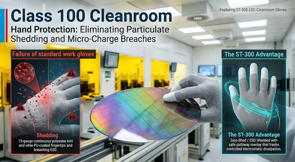
Dust suppression and high-purity reflow soldering assurance: The fiber ends of ordinary fabric gloves are prone to fraying and shedding under repeated friction and bending. Submicron-sized debris that falls off and mixes into the reflow solder paste can cause porosity and cold solder joints. The ST-310’s palm-covering polymer resin structure fully encapsulates the fingertips and palm—areas prone to mechanical wear—eliminating contamination from glove fabric lint while meeting the Helmke Drum ultra-low dust emission standard.
Human-Machine Touch Interaction & Cleanroom Operational Continuity
On modern SMT production lines, where automotive electronics and the Industrial Internet of Things are widely adopted, operators’ work interfaces have long gone beyond traditional, purely manual component insertion and mechanical assembly. From feeder calibration on placement machines and re-inspection via AOI optical inspection to fine-tuning parameters on functional test stations (FCT) and data entry into the MES system, digital interaction via the human-machine interface (HMI) permeates the entire manufacturing cycle. If anti-static gloves fail to balance capacitive touch responsiveness with microclimate regulation for perspiration, they will directly disrupt the continuity of digital processes and may even pose a fatal risk of electrostatic discharge due to frequent, non-compliant removal of gloves.
Capacitive Touch Screen Compatibility Without Glove Removal
Industrial-grade production equipment commonly uses projected capacitive touchscreens (PCT), whose sensing principle relies on changes in capacitive reactance caused by minute charge coupling between the fingertip and the screen’s electrode array:
The Vicious Cycle of Touch Failure Caused by Non-Conductive Gloves: Traditional non-conductive safety gloves or low-end, thick, rubber-coated gloves create a wide, thick physical insulating barrier between the back of the hand and the fingertips, completely blocking the transmission of the body’s weak high-frequency AC signals and causing the capacitive screen to become unresponsive. To enter work orders or reset alarms on machinery, operators often subconsciously and frequently remove their gloves to operate the screen with bare fingers. This non-compliant behavior instantly disrupts the closed-loop grounding circuit in the Electrostatic Protection Area (EPA), causing the operator’s bare hands to rapidly accumulate thousands of volts of high voltage in the dry airflow. When the operator re-contacts precision circuit boards, this directly causes electrostatic discharge from bare hands to sensitive chips;
Capacitive Coupling Response of the 3D Carbon Mesh and Microporous Polyurethane: The ST-310 utilizes a homogeneous, co-woven network of nanoscale conductive carbon fibers to create high-density, three-dimensional conductive pathways across the fingertips and palms of the gloves. The specialized conductive microporous polyurethane layer coating its surface not only offers excellent flexibility but also possesses superior charge coupling and conduction properties, enabling the precise and instantaneous mapping of faint microampere-level capacitive disturbance signals from the fingertips to the surface of industrial capacitive touchscreens, thereby achieving extremely high-sensitivity touch feedback (Touch Screen Compatible);
This ensures operational continuity and production rhythm in cleanroom environments: by supporting direct touchscreen operation without removing gloves, it eliminates the dispersion of skin flakes, oils, and microparticles into the air caused by repeatedly putting on and taking off gloves, thereby strictly adhering to ISO cleanroom dust control standards; At the same time, by eliminating the redundant step of putting on and taking off gloves, it enables seamless, second-level transitions between clearing equipment alarms, fine-tuning parameters, and PCBA turnaround assembly, significantly increasing the hourly production output (UPH) of high-speed SMT production lines.
Breathability and Sweat Electrolyte Management
During an 8-hour shift of high-intensity work, the palms—one of the body’s areas with the highest concentration of sweat glands—play a critical role in regulating the hot and humid microclimate. This regulation directly affects the electrical and physical baseline of electrostatic protection materials:
Mechanism by which sweat electrolyte permeation disrupts impedance balance: Conventional fully enclosed rubber-coated gloves or thick gloves with extremely poor breathability easily trap the hands in a hot and humid “stuffy greenhouse” environment. When sweat accumulates on the palms for extended periods, the large amounts of strong electrolyte ions—such as sodium chloride (NaCl) and lactic acid—contained in the sweat gradually seep into and permeate the interior of the glove fabric fibers. The disordered accumulation of electrolyte ions disrupts the originally precisely calibrated volume resistivity balance of the glove lining, causing a nonlinear drop in local point-to-point resistance—which may even fall below the safety threshold of 1.0 × 10⁵ ohms. This degrades the originally controlled electrostatic dissipation layer into a hazardous, conductive, hard-grounded layer; contact with a charged workpiece will immediately trigger a transient high-current discharge;
13-gauge open-weave construction and back-side directed thermal convection: The ST-310 incorporates the concept of active microclimate engineering into its structural design, retaining a 13-gauge, uncoated, mesh-like open-weave structure made of high-density filament polyester on the back of the hand (13-gauge seamless liner). The gaps in the fabric provide high-flux microporous channels for free air convection, enabling the continuous, directed removal of heat and moisture emitted from the skin’s surface to the external environment by utilizing the micro-airflow generated by hand movement;
Unidirectional breathability and water-blocking properties of the microporous polyurethane on the palm: The polymer polyurethane coating covering the palm features a dense, interconnected honeycomb microporous structure. The pore diameters are significantly larger than the diameter of gaseous water vapor molecules but much smaller than liquid water droplets, allowing sweat vapor from the palm to rapidly penetrate the coating and dissipate outward, keeping the palm dry and fresh. This superior microclimate management prevents sweat from condensing into a liquid water film on the palms, ensuring that the glove’s surface resistivity and system resistance to ground remain consistently stable within the optimal safety range of 1.0 × 10⁶ to 1.0 × 10⁸ ohms throughout the entire shift.
Standardized Quality Verification: ANSI/ESD S20.20 & In-Line Audit SOP
In automotive-grade SMT manufacturing and industrial control electronics electrostatic protection areas (EPAs), anti-static gloves must never be used directly on the production line as untested, ordinary personal protective equipment (PPE). To ensure the reliability of the entire electrostatic discharge (ESD) system, production line Quality Assurance (QA) and ESD protection engineers must establish standardized, reproducible procedures for incoming material inspection and in-line production line audits. By strictly enforcing internationally recognized testing standards to quantitatively verify the gloves’ system grounding impedance and resistance to drift under extreme environmental conditions, potential risks of chip breakdown caused by batch-specific impedance anomalies can be thoroughly mitigated.
Resistance-to-Groundable Point (Rgp) System Testing
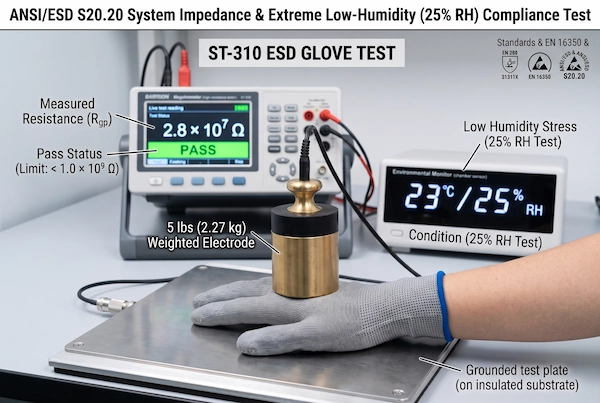
Simply measuring the in-vitro point-to-point resistance of glove fabric cannot fully replicate the actual system discharge conditions experienced by workers while wearing gloves. In accordance with the ANSI/ESD S20.20 and International Electrotechnical Commission (IEC) 61340-5-1 standards, production line acceptance must include a comprehensive evaluation of the resistance to a groundable point (Rgp) while the gloves are being worn:
Standard Test Equipment and Weight Specifications: Testing must be performed using a calibration-grade high-resistance meter (megohmmeter) that complies with standard specifications, equipped with a standard weight electrode—the total weight of the electrode must be strictly calibrated to 5 pounds (approximately 2.27 kilograms), with a conductive rubber pad (63.5 mm in diameter) having a Shore A hardness of 50 to 70 degrees laid on the base to simulate a constant gravitational contact stress;
Dynamic Measurement Procedure for the Human-Machine Grounding System:
The tester wears the gloves to be tested in accordance with regulations within a temperature- and humidity-controlled testing chamber and establishes a low-impedance physical connection to the workshop’s common grounding point (Groundable Point) via a compliant, grounded antistatic wrist strap;
The tester places the palm of the gloved hand completely flat against an insulation test substrate that has been cleaned with anhydrous ethanol;
A 5-pound hammer electrode is pressed vertically and steadily onto the center of the glove’s palm or the key stress contact area at the fingertips, ensuring that the test probe’s contact surface fully engages with the glove’s microporous coating. A constant DC test voltage of 10 V (for low-resistance mode) or 100 V (for high-resistance mode) is applied;
After maintaining the voltage for 15 seconds, read the stable resistance value from the meter;
System pass/fail criteria and discharge safety threshold: The system’s total impedance (Rgp)—measured from the operator’s skin through the carbon fiber conductive mesh inside the glove to the grounded terminal—must remain strictly within the range of 1.0×10⁶ to 1.0×10⁸ ohms. A resistance value exceeding 1.0×10⁸ ohms is deemed to indicate excessive dissipation delay, while a value below 1.0×10⁶ ohms is deemed to pose a risk of hard discharge surges; in both cases, the entire batch must be rejected and intercepted.
Low-Humidity Pre-Conditioning Protocol (25% RH Testing)
In cleanrooms located in northern regions during winter or those exposed to extremely dry air currents, the relative humidity (RH) of the workshop environment often drops sharply to 25% or even lower. Many low-quality anti-static gloves that rely on moisture activation in the air experience an exponential increase in resistance under dry conditions, effectively degrading into high-insulation materials. Therefore, it is essential to implement the extreme low-humidity pre-conditioning test protocol specified in European Standard EN 16350:
24-hour pre-conditioning in an extreme low-humidity environmental chamber:
Remove the batch of ST-310 gloves to be tested from their original sealed packaging and lay them flat inside a precision environmental test chamber;
The chamber temperature is strictly controlled at 23 degrees Celsius (tolerance: ±1 degree), and the relative humidity is precisely reduced to 25% RH (tolerance: ±3%);
The glove samples are continuously exposed to this extremely dry, moisture-free environment for at least 24 hours to thoroughly remove all non-bound free water molecules from the fibers;
Immediate in-situ vertical resistance (Rv) and surface resistance testing:
Upon completion of the conditioning cycle, the operator must perform a re-test of electrical properties either through the designated glove port on the test chamber or within 3 minutes of removing the sample;
Use concentric ring electrodes and cylindrical electrodes to perform multi-point impedance measurements on the rubber-coated palm, fingertips, and back of the hand areas, applying a 100 V DC high-voltage electric field;
Engineering Baseline for Resistance to Impedance Drift: The tested ST-310, featuring a continuous network of microscopic nano-carbon fiber filaments throughout the inner liner, does not rely on surfactants to adsorb ambient moisture. After undergoing a 24-hour 25% RH extreme drying test, its measured surface resistivity and vertical resistance remained stable within the compliance limit of less than 1.0 × 10⁸ ohms, demonstrating excellent weather resistance and resistance to impedance drift, and meeting the admission requirements for seamless, continuous operation in automotive electronics workshops throughout all seasons.
Implementation Guide: Upgrading ESD PPE Protocols on Automotive SMT Lines
Upgrading anti-static personal protective equipment (PPE) for hands in automotive electronics production facilities—from traditional, unbranded work gloves or ordinary anti-static consumables to standardized, automotive-grade, controlled PCB assembly anti-static work gloves—is by no means a simple matter of replacing materials through procurement. Rather, it is a systematic engineering effort involving process sensitivity calculations, workstation electrostatic exposure risk assessments, and quantitative yield tracking. The automotive industry’s stringent requirements for “zero defects” and long-term traceability dictate that process engineering (PE) and quality departments must adopt a phased, data-driven implementation approach to ensure that every human-machine interaction is traceable.
Workstation Audit & Critical Component Mapping
The first step in upgrading the protection system is to establish a tiered protection audit map based on component electrostatic sensitivity (ESDS) throughout the entire process in the Electrostatic Protected Area (EPA):
Scan of Core Electrostatic-Sensitive Device (ESDS) Distribution: The process team must collaborate with hardware design and component engineering departments to conduct a comprehensive review of the PCB layouts for automotive ECUs, BMS, and domain controllers, with a focus on identifying high-voltage-differential linear regulators (LDOs), power MOSFETs with extremely thin gate oxides, high-sensitivity CAN/LIN bus transceivers, and pre-driver ICs without built-in robust ESD protection. Identify the physical exposure points of these sensitive chips’ exposed pins on the assembly line;
Calculation of Mechanical Contact Stress and Charge Exposure at Workstations: Use an electrostatic field tester and a non-contact electrostatic voltmeter to measure the friction voltage baseline at each assembly node one by one:
High-risk electrostatic charging operations: the feeder intake port of the SMT placement machine; manual visual inspection and re-inspection points during Automated Optical Inspection (AOI); the clamping area of the ICT test fixture after reflow soldering; and workstations where PCBA boards are manually pushed into metal shielded enclosures. These operations involve frequent workpiece movement and high mechanical shear forces, making them particularly prone to uncontrolled triboelectric charging;
Medium-to-low-risk handling operations: Post-production processes such as palletizing finished product cartons and labeling outer boxes;
Implement a tiered technical access matrix: For high-risk static-generating operations and the assembly of heavy, thick-copper-clad board assemblies, the use of ST-310 anti-static gloves with full-palm immersion coating is mandatory to ensure stable, large-area grounding and slip resistance; Conversely, for highly cleanroom-sensitive operations such as localized dispensing on bare chips or lens module assembly, finger-dipped or ultra-thin specialty gloves are provided to establish a precise, context-specific protection hierarchy.
Two-Stage PPE Rollout and Yield Tracking SOP
To prevent production line adaptation issues or operational resistance caused by large-scale, one-size-fits-all replacements, companies should implement a standardized two-stage rollout procedure (Two-Stage Rollout):
Stage 1: Small-Batch Controlled Validation at High-Risk Pilot Stations (Pilot Trial):
Selection of pilot stations: Prioritize key stations with historically high yield volatility and the highest frequency of “unexplained chip failure” in rework statistics—such as the manual feeder station on SMT feeders and the loading/unloading sections of automotive motherboard functional testing (FCT);
Establish a 14-day comparative baseline: During production of the same model and work orders, set up two control production lines: Line A maintains the original tools, while Line B strictly switches to ST-310 gloves. Each day during shift handoffs, ESD specialists used a high-resistance meter and a hammer electrode to measure and record the human-machine system grounding resistance (Rgp) of operators wearing gloves, thereby creating a comprehensive electrical compliance log;
Phase Two: Full-Line Implementation and Monitoring of Key Yield Parameters (FPY):
First-Pass Yield (FPY) vs. Early Failure: Dynamically track the First-Pass Yield (FPY) for FCT functional testing via the MES system. Following the introduction of automotive-grade gloves featuring a homogeneous conductive carbon mesh and a microporous polyurethane coating, focus on comparing the reduction in rework data—such as “excessive leakage current” or “sporadic output logic disruptions”—caused by micro-breakdowns in MOSFET gates;
Cross-Validation of Solder Mask Adhesion and Solder Joint Void Rate: PCBA units from a pilot production line were randomly sampled after cleaning and solder mask application. Using a microscopic endoscope and X-ray inspection, we verified whether the absence of sulfur and silicone oil coatings eliminated solder mask bubbles, pinholes, and poor solder joint wetting during reflow soldering;
Establishment of a standardized Standard Operating Procedure (SOP): After confirming a steady improvement in the FPY metric and the elimination of mechanical impact damage to individual boards, the validated glove specifications were formally incorporated into the production process control document (Control Plan) and rolled out across all anti-static assembly lines throughout the factory, completing a closed-loop upgrade of process protection standards.
Frequently Asked Questions (FAQ)
Why are palm-coated ESD gloves preferred over finger-tipped gloves for handling automotive PCBAs?
At automotive electronics assembly stations, printed circuit boards (such as engine ECUs, battery management systems (BMS), and in-vehicle infotainment headsets) typically incorporate large-area, multi-layer, thick copper traces, metal heat-dissipation shields, and heavy-duty high-voltage connectors. The physical weight of these boards is significantly greater than that of consumer smartphone motherboards:
Grip Torque and Fatigue-Resistant Support: Finger-tipped gloves are coated only on the fingertips. When operators handle heavy boards or large-sized boards with side lengths exceeding 20 centimeters, they can only rely on the weak gripping force of their fingertips to maintain balance. Under high-speed assembly line rhythms, insufficient friction at the fingertips can easily cause boards to slip out of the operator’s hands, resulting in broken MLCC ceramic capacitors or shattered high-voltage connector latches. The ST-310, featuring full-palm dipping, utilizes a microporous polyurethane (PU) layer that covers the entire palm and fingertips to generate sufficient static and dynamic surface friction. This allows operators to support large circuit boards with their palms, eliminating the risk of fatigue-induced slippage and drops;
The physical grounding contact area is significantly increased: Automotive-grade PCBA peripherals are typically designed with a wide outer ring of protective grounding copper foil (Chassis Ground). When operators support the bottom of the board with both hands, the full-palm coating design establishes a large physical contact surface with the board’s grounding area and the workstation’s anti-static mat. Compared to the millimeter-scale point contacts provided by finger-dipped gloves, full-palm contact significantly reduces the equivalent contact resistance at the charge dissipation interface, shortening the time required to dissipate triboelectric charges to within milliseconds and establishing a more robust barrier for smooth charge diversion.
How does a latent ESD defect in a MOSFET gate oxide pass final end-of-line testing?
The most critical characteristic of a MOSFET gate oxide (SiO₂) that has been subjected to a weak electrostatic discharge (ESD) is its “latent nature”:
Microscopic dielectric breakdown and leakage current remain within acceptable limits: When low-voltage static electricity accumulated from factory workers walking or handling materials—such as micro-arcs ranging from 50 V to 100 V—is injected into the chip’s pins, the energy is insufficient to instantly sever internal metal bonding wires, nor does it directly and completely melt through the nanometer-thick SiO₂ dielectric to form a low-resistance short-circuit path; Instead, it typically only excites localized electron traps and submicron-scale lattice damage pinholes at weak points in the gate. During in-circuit testing (ICT) and functional testing (FCT) conducted at room temperature on the production line, although the chip’s static gate leakage current (I_gss) is slightly higher than that of undamaged devices, the increase is so minimal (typically still within the microampere or even nanoampere range) that it falls well within the allowable tolerance range specified in the factory technical specifications, allowing the chip to easily pass testing and be classified as a qualified product;
Accelerated thermoelectric degradation under harsh in-vehicle operating conditions: Once an automotive electronic control unit containing this latent defect is installed in a vehicle and delivered, the operating environment abruptly shifts to severe dynamic loads—including sustained high temperatures of 85 to 125 degrees Celsius in the engine compartment, mechanical vibrations caused by road bumps, and reverse voltage spikes generated by the frequent switching of inductive loads. High temperatures and strong electric field stresses cause severe electromigration and localized heat concentration at the originally damaged micro-pores, causing minor defects to rapidly deteriorate into irreversible short-circuit melt holes with complete breakdown. This ultimately leads to the sudden failure of critical electronic control functions while the vehicle is in motion.
Does the ST-310 glove maintain static dissipation in low-humidity winter workshops?
It is fully capable of maintaining consistent, compliant electrostatic dissipation performance:
Principle of intrinsic carbon fiber filament conductivity: Low-cost anti-static gloves commonly found on the market typically rely on spraying hygroscopic surfactants onto the surface of ordinary fabrics, and their conductive pathways depend entirely on moisture molecules in the air; Once winter sets in in northern regions or when high-airflow air conditioning cycles are activated in cleanrooms—causing the relative humidity (RH) to plummet below 25%—these gloves cannot absorb sufficient moisture. As a result, their surface resistance increases exponentially to over 1.0×10⁹ ohms, completely losing their antistatic protection;
Continuous physical carbon mesh independent of ambient humidity: The ST-310 features a composite interwoven liner made of 13-gauge continuous polyester filaments and nano-scale bicomponent conductive carbon fibers (13-gauge seamless Carbon/Polyester liner). Its charge dissipation pathway relies entirely on the inherent high-conductivity carbon particle crystal network within the fibers, constituting purely physical free-electron transition conduction; Consequently, even after undergoing a rigorous 24-hour pre-conditioning test (in accordance with the EN 16350 standard) under extremely dry conditions of 25% RH, the glove’s point-to-point resistance and resistance to ground remain strictly within the optimal dissipation range of 1.0×10⁶ to 1.0×10⁸ ohms, demonstrating exceptional all-weather stability.
Will palm-dipped PU coatings interfere with the adhesion of conformal coatings on circuit boards?
They will absolutely not negatively affect the adhesion of conformal coatings:
Eliminates contamination from silicone release agents and free sulfur: Traditional, low-end dip-molded gloves commonly contain silicone-based lubricants or sulfur-containing cross-linking agents added during the molding and resin polymerization processes. Upon contact with the PCB surface, these low-molecular-weight organosiloxanes rapidly migrate and deposit on the epoxy solder mask, forming an extremely thin, low-surface-energy, hydrophobic contaminant film. When the board undergoes the subsequent conformal coating application process, the contaminated areas cannot be fully wetted by the resin-based coating, leading to widespread bubbles, pinholes, mottling, and delamination (peeling) in the cured conformal coating film during cross-hatch adhesion testing;
Automotive-grade high-purity polyurethane standards: ST-310 utilizes a silicone-free, sulfur-free, pure water-based polyurethane composite formulation specifically developed for high-precision microelectronics manufacturing. Before shipment, it undergoes a multi-stage deep cleaning and drying process using industrial-grade high-purity deionized water (DI Water). The microporous polymer layer on the glove surface is chemically extremely stable and does not leach volatile organic plasticizers. During assembly operations, it leaves no hard-to-clean chemical residues or ionic particles on the circuit board surface, thereby fully preserving the original surface free energy of the solder mask layer. This ensures that the acrylic, polyurethane, and silicone triple-protection coatings can form a dense, smooth, and highly adhesive insulating protective passivation layer.
Closing & Engineering Specification Advisory
In manufacturing facilities for new energy vehicles, rail transit, and high-voltage industrial control electronics, protecting sensitive semiconductor devices presents a system-level engineering challenge. Even the slightest static electricity generated by operational friction can create irreversible risks of premature breakdown within the chip’s insulating dielectric, which is measured in nanometers. To truly eliminate sudden quality risks caused by electrostatic damage, companies must break away from the inertia of vague procurement practices for traditional protective consumables and comprehensively incorporate impedance control at the human-machine interface, anti-slip torque, and chemical cleanliness metrics into a standardized quality control system (Control Plan).
As a PCB assembly antistatic work glove that mmeetsstringent automotive-grade standards, the ST-310 features a continuously woven, highly conductive carbon fiber 3D topological framework, a full-palm polymer microporous anti-slip coating, and a strictly controlled electrostatic dissipation window of 1.0×10⁶ to 1.0×10⁸ ohms. It provides a stable and smooth charge dissipation path and physical protection against drops for automotive ECUs, BMS units, and large-format industrial control motherboards. For more detailed information on this product’s certification for ANSI/ESD S20.20 system grounding impedance, EN 16350 extremely low humidity testing, to obtain ion chromatography and FTIR silicone-free cleanliness test reports, or to request production line validation samples for your company’s high-risk SMT assembly stations, please visit the ST-310 Antistatic Work Glove dedicated engineering specifications and sample request page.