

Introduction: The Hidden Physics of Electrostatic Charge Decay in Cleanroom Assembly
When evaluating cleanroom contamination control and ESD reliability, antistatic gloves surface resistance testing directly determines the actual upper limit of the entire production line’s protection against electrostatic overstress (EOS) and microscopic charge decay failures in precision electronics assembly. However, quality control engineering teams at many high-tech manufacturing companies have long faced a hidden, seasonal failure cycle: when anti-static work gloves from the same batch are inspected upon arrival during the hot and humid summer months, their surface resistance is well within the acceptable range; yet once the winter heating season begins or in dry northern environments—when the relative humidity in cleanrooms plummets below 30%—unexplained potential electrical breakdown failures begin to occur frequently in MOS gate oxides and high-sensitivity integrated circuits on the production line.
The root cause of these seasonal quality incidents lies in the fact that traditional procurement and quality inspection practices overlook the microscopic physical nature of material charging and charge dissipation. A large number of low-cost anti-static gloves on the market are essentially “insulating fabrics”; their feeble appearance of conductivity relies entirely on hygroscopic quaternary ammonium salt surfactants that are soaked into or sprayed onto the surface. When ambient humidity is high, these chemical coatings adsorb free water molecules from the environment to form a temporary hydrated ionic film, thereby yielding a false low-impedance reading in routine testing. Once the ambient humidity is drawn out by a drying air conditioning system, this hydrated film rapidly dehydrates and breaks down. The original ionic pathways are instantly severed, causing the glove’s surface resistance to skyrocket to 10^11 ohms or higher, completely degrading it into a high insulator. When operators frequently pick up wafer trays or insert and remove flexible printed circuits (FPCs) at their workstations, molecular contact and separation at the microscopic level can instantly accumulate thousands of volts of electrostatic potential. If this potential comes into contact with microchip pins, it will directly break down the internal nanoscale dielectric layer via uncontrollable nanoscale hard discharge pulses.
To eliminate the hidden risks of electrostatic breakdown in dry, low-humidity environments at their source, the quality engineering team must look beyond the illusions of static testing and establish a framework for understanding charge dissipation based on the inherent physical properties of materials. Anti-static equipment that truly meets modern microelectronics cleanroom standards must abandon speculative processes that rely on externally applied chemical coatings and instead rely on three-dimensional, continuous charge dissipation pathways built within the fabric using micron-scale composite conductive filaments. Regardless of how drastically external air humidity fluctuates, this intrinsically conductive structure can smoothly induce a safe and controlled decay of charges to ground within microseconds, eliminating the accumulation of localized charge islands. For technical and procurement managers currently investigating the sources of electrostatic breakdown on production lines and seeking to restructure cleanroom electrostatic discharge (ESD) control procedures, we recommend first systematically reviewing our industrial anti-static technology framework: Antistatic (ESD) Gloves.
Triboelectric Kinetics: Charge Transfer at Contact-Separation Interfaces
In a cleanroom environment, the generation of electrostatic charges is not an elusive, random event, but rather an inevitable reaction that strictly follows the laws of solid-state physics and materials thermodynamics at interfaces. When troubleshooting ESD anomalies on production lines, many quality and process engineers often intuitively assume that only high-speed sliding friction can generate high-voltage static electricity; however, in nanoscale microelectronics assembly scenarios, the microscopic interactions between the polymer outer layer of gloves and the surface of workpieces are far more intense than macroscopic friction. To truly grasp the core physical significance of antistatic glove surface resistance testing, one must first analyze the microscopic charge transfer and material polarization kinetics at contact interfaces.
The Triboelectric Series and Interface Polarization
From the perspective of solid-state physics, the charge transfer that occurs when two different materials come into contact is essentially a quantum mechanical process driven by differences in the Fermi levels or mismatches in the effective work functions at the interface between the two materials:
Band alignment and electron drift at the moment of contact: When the polymer substrate of the glove (such as polyurethane [PU] or polyester fiber) physically adheres to the workpiece surface, the electron clouds on the surfaces of the two materials overlap; To achieve thermodynamic equilibrium between the electrochemical potentials (Fermi levels) on either side of the interface, electrons spontaneously tunnel unidirectionally across microscopic potential barriers from the material with the lower work function (weaker electron binding) and drift to the surface of the material with the higher work function (stronger electron affinity);
Polarity divergence of workpiece materials in the triboelectric series: In the standard triboelectric series, polyurethane (PU) typically occupies a relatively positive position; When a worker wearing PU-coated gloves touches a polytetrafluoroethylene (PTFE) carrier or a fluoroplastic tray located at the most negative end of the series, electrons on the glove’s surface undergo large-scale outward migration, leaving a large number of positive charge holes on the glove’s surface; Conversely, when the gloves come into contact with anodized aluminum fixtures or copper nozzles—surfaces rich in unbound electrons—the metal’s extremely high electron mobility causes the glove surface to rapidly capture free electrons, resulting in a strongly negative charge;
Charge capture at the interface between epoxy resin PCB substrates and gloves: During the handling of FR-4 epoxy resin circuit boards—the most common type on SMT production lines—when the polar groups on the epoxy resin molecular chains come into contact with the polymer coating layer of the gloves, microscopic dipoles at the interface align in a specific direction, inducing severe interfacial polarization; Since the glove itself lacks a continuous, physically conductive network to dissipate this charge outward, this microscopic charge migration remains trapped directly at the fingertips and on the surface of the palm, forming localized regions of extremely high charge density.
Contact-Separation vs. Frictional Dynamics
In modern fully automated and semi-automated precision assembly stations, the vast majority of static charges that cause component damage do not result from violent physical scraping, but rather from millisecond-scale microscopic “contact-separation” mechanical cycles:
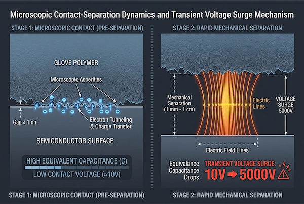
Atomic-level contact at microscopic contact points: Any wafer surface or glove-coated surface that appears extremely smooth is, under microscopic examination, covered with undulating microscopic asperities; When a worker gently pinches the edge of a chip or picks up a flexible printed circuit board (FPC), external forces cause the glove polymer to undergo elastic deformation and tightly conform to the microscopic asperities on the workpiece surface, reducing the contact gap to the nanometer scale (less than 1 nanometer). At this point, interface charges redistribute at an extremely high flux driven by contact pressure;
A voltage surge caused by a sudden drop in capacitance upon mechanical separation: According to the classical physical relationship for parallel-plate capacitance, capacitance is inversely proportional to the distance between the plates, while voltage equals the charge divided by the capacitance value; in the contacted state, the gap between the two interfaces is extremely small, and the system’s interfacial capacitance is extremely large. At this point, even if a large amount of transferred charge has accumulated, the interfacial voltage typically remains within a safe range of tens of volts; However, when a worker’s finger lifts the workpiece and the two surfaces instantly lose contact, the interfacial gap expands from the nanometer scale to the millimeter or even centimeter scale within microseconds, causing the system’s equivalent interfacial capacitance to plummet by tens of thousands of times;
A physical surge of transient electrostatic peaks reaching thousands of volts: Since microscopic charges on insulating materials cannot rapidly flow back to their original positions at the moment of separation, and given the physical constraint that the total charge remains essentially constant, the instantaneous, precipitous drop in system capacitance directly forces a sudden surge in local electrostatic potential; Even during an extremely gentle grasp-and-release motion with no macroscopic friction, the transient open-circuit electrostatic voltage at the fingertip contact area can directly exceed 2,000 to 5,000 volts; this invisible high-voltage static electricity trapped on the fingertip surface is ready to release a lethal, destructive arc the next time it comes into proximity with a metal pin.
Dehydration Breakdown of Topical Surfactant Films
To suppress the high potential generated by the aforementioned contact-separation phenomenon, many commercially available standard anti-static gloves attempt to create a conductive layer using a low-cost “chemical surfactant coating method.” However, this approach has a fatal structural flaw under the physical conditions of a cleanroom:
Relying on the illusion of hydrophilic ionic conductivity from ambient water molecules: During production, these inexpensive gloves are simply immersed in or sprayed with hydrophilic surfactants such as quaternary ammonium salts, fatty acid esters, or alcoholamines; Their anti-static mechanism relies entirely on the exposed polar groups of hydrophilic molecular chains—these groups adsorb trace water molecules suspended in the cleanroom air, forming an extremely fragile hydrated ionic layer, only a few molecular layers thick, between the glove fibers and the coated surface;
The hydrated film dehydrates and breaks down due to dry airflow: during winter or when the cleanroom’s fresh air system operates continuously at high intensity, the concentration of free water molecules in the indoor air is extremely low (relative humidity is often below 25%); Driven by a partial pressure gradient of water vapor, the hydrated ionic layer on the glove surface—which was already loosely adsorbed—undergoes severe physical dehydration and evaporative desorption; as the free water molecules supporting ion movement rapidly dissipate, the original continuous electrolyte ion pathways dry up, fracture, and shatter within a few hours;
Complete degradation of the physical insulating state and a sudden discharge surge: The instantaneous collapse of the chemically hydrated network directly severs the lateral and longitudinal charge dissipation pathways on the glove’s surface; at this point, the glove’s actual surface resistivity rises exponentially, spiraling out of control from the initially inspection-qualified 10⁸ ohms to over 10¹¹ ohms, causing the glove to completely degrade into a highly insulating polymer; When unsuspecting assembly personnel continue to handle highly sensitive MOSFETs or chip pins in a dry environment, the high-voltage charges generated by contact and separation become trapped on the parched glove surface. Eventually, these charges discharge intensely upon contact with exposed pads, triggering batch-wide wafer breakdown and scrapping.
Material Impedance Spectrum: Insulative, Dissipative, and Conductive Regimes
In industrial electrostatic discharge (ESD) engineering, the impedance properties of gloves are not simply a binary distinction between “conductive” and “non-conductive,” but rather span a continuous spectrum of polymer electrical properties covering more than a dozen orders of magnitude. Many procurement and quality control teams are prone to falling into a black-and-white misconception when establishing incoming material standards: they either mistakenly distribute highly insulating gloves as ordinary dust-proof gloves directly to critical production lines, or blindly pursue purely conductive materials with extremely low impedance. In fact, the rate of charge movement is strictly governed by the material’s intrinsic resistivity; any extreme material that deviates from the scientifically defined impedance window can trigger catastrophic physical failures at precision semiconductor workstations. To truly establish a robust ESD barrier, process engineers must deeply understand the three major physical zones within the material impedance spectrum.
The Insulative Danger Zone (> 1.0 x 10^11 Ohms)
When the surface resistance or volume resistance of a protective glove exceeds 1.0 x 10^11 ohms, the material has, by the definition of solid-state physics, fully entered the high-insulator range:
Microscopic charge traps and carrier freezing effects: In ordinary pure polyester, nylon filaments, and unmodified polyurethane (PU) coatings, there are virtually no delocalized electrons or free ions capable of free movement within the molecular chains; When these materials accumulate triboelectric charges through contact and separation, their internal conductivity approaches zero, causing electrons to become firmly trapped in localized molecular defects and surface energy level traps, unable to diffuse outward or be conducted into the ground along the thickness direction;
Hazards of long-term retention of strong localized electric fields and electrostatic adsorption: Static charges trapped at the fingertips of insulated gloves cannot spontaneously neutralize and often remain stable in dry air for hours or even days; This localized, high-density charge accumulation generates an extremely strong electrostatic field within a space of tens of micrometers around the glove. Not only does this continuously and forcibly attract submicron-sized airborne particles in the cleanroom—completely compromising the local Class 100 cleanliness—but it also induces sustained charge induction in surrounding sensitive components;
Non-contact Field-Induced Electrostatic Breakdown (CDM Failure Model): The most catastrophic damage often occurs the instant before physical contact takes place; when an operator wearing insulated gloves approaches a sensitive chip mounted on an assembly fixture, the localized strong electric field on the glove’s surface forces the conductors inside the chip to generate intense electrostatic induction and induce polarization; Once the chip’s pins subsequently come into contact with a grounded metal test fixture, the induced and confined charges inside the chip will instantly discharge toward ground at extremely high speeds on the order of nanoseconds, directly triggering a charged-device model (CDM) discharge and causing avalanche breakdown in the ultra-thin dielectric layer—which is only a few nanometers thick—inside the chip.
Hazards of Hard Discharges in Conductive Materials (< 1.0 x 10^5 Ohms)
In response to the hazards associated with insulating materials, some engineers tend to swing to the other extreme, believing that “since insulating materials accumulate charge, gloves with lower resistance and higher conductivity are safer.” However, the reality is quite the opposite: purely conductive gloves with a resistance below 1.0 × 10⁵ ohms also pose significant hidden risks in electronics manufacturing:
Avalanche-like Transient Hard Sparking Inducing Melt-Through Breakdown: When the resistance of the glove material is too low, the rate at which it discharges charge is extremely fast. When a human body or a charged workpiece carrying a static potential of several thousand volts comes into contact with an ultra-low-resistance glove, the charge is no longer released gradually but instead undergoes an avalanche-like instantaneous hard sparking within an extremely short timeframe—ranging from a few tenths of a nanosecond to several nanoseconds; This process instantly releases transient peak surge currents as high as several amperes or even tens of amperes;
Thermal burnout of metal interconnects caused by electrical overstress (EOS): Although the total electrical charge released during hard sparking is extremely small, the extremely short duration results in an extremely high peak power density; When such intense transient high currents pass through microchip pins and nano- to micro-scale metal interconnects, they instantly generate a strong localized Joule heating effect, directly causing the aluminum or copper interconnects inside the microchip to melt and vaporize, or forming permanent micrometer-scale micro-craters and ablation-induced short circuits on the surface of the silicon substrate;
Electric Shock Hazards and Personal Safety Red Lines at Live Testing Stations: On production lines with DC or AC live testing stations (such as SMT in-line live testing, industrial power module final assembly, and power battery module wiring), exposed test probes or flat cables often carry operating voltages ranging from tens to hundreds of volts; If an operator wears conductive gloves with a resistance lower than 1.0 × 10⁵ ohms, and accidentally touches a live rail, the gloves will lose their current-limiting impedance function and act as bare copper wires. The external operating current will then flow unimpeded through the gloves, through the operator’s body, and into the ground terminal, causing severe arcing or even life-threatening electric shock accidents.
The Optimal Dissipative Window (1.0 x 10^6 to 1.0 x 10^9 Ohms)
The core philosophy of electrostatic protection engineering in microelectronics is “controlled discharge,” rather than “brute-force short-circuiting.” Through rigorous physical analysis, the materials science community and international industrial standards have established the range of 1.0 × 10⁶ to 1.0 × 10⁹ ohms as the golden static dissipative window (Static Dissipative Regime) for glove design:
Millisecond-scale, gradual charge decay pathway: Materials within the 1.0 × 10⁶ to 1.0 × 10⁹ ohm impedance range possess a precisely controlled microscopic conductive topological structure; When static charges are generated on the surface of the human body or a workpiece, this impedance range provides a continuous, unobstructed discharge path, forcing the charge to flow smoothly to ground within a few milliseconds to tens of milliseconds. This ensures that static charges do not accumulate at the fingertips to form a high-voltage electric field, while also eliminating the destructive transient surge current peaks caused by nanosecond-level hard discharges;
Built-in bidirectional current-limiting safety valve mechanism: From the perspective of circuit equivalence, a lower impedance threshold of 1.0 × 10⁶ ohms (1 megohm) or higher establishes a constant, high-precision current-limiting resistor in series between the human body and the workstation; Even in the event of accidental leakage currents in the hundreds of volts or insulation failure in equipment housings, Ohm’s Law ensures that the leakage current flowing through the glove and penetrating the finger is firmly limited to the microampere range (below both the human perception threshold and the electric shock hazard threshold), thereby achieving a two-way physical balance between the safety of microchip devices and the occupational health of front-line workers;
Mandatory benchmark consensus of the International Organization for Standardization (ISO): This optimal impedance range has been fully adopted by mainstream international ESD control standards; whether it is the European standard EN 16350, which stipulates that vertical resistance must be strictly less than 1.0 × 10⁸ ohms, or the North American standard ANSI/ESD S20.20, which requires that the upper limit of system-level grounding resistance be less than 1.0 × 10⁹ ohms, the underlying physical principle in both cases is to firmly anchor the glove material within this controlled dissipation range, resolutely eliminating high-insulation risks exceeding 1.0 × 10¹¹ ohms and high-discharge risk zones below 1.0 × 10⁵ ohms.
Charge Decay Dynamics: Quantifying Dissipation Velocity Under FTMS 101C
When evaluating the electrical performance of anti-static gloves for cleanrooms, static resistance testing alone reflects only the material’s ohmic conductivity under a specific DC voltage and cannot fully reveal the dynamic charge dissipation behavior observed on actual production lines. In modern automated semiconductor assembly and precision electronics manufacturing, cycle times are often measured in milliseconds, with front-end workers completing material pickup, transfer, and placement in an extremely short period. If gloves possess only theoretical low impedance but fail to discharge friction-induced charges at a sufficiently high physical rate before contacting microscopic components, residual voltage will still cause electrostatic stress breakdown at the moment of contact. Therefore, quantifying the rate of charge dissipation through Static Decay Kinetics is an indispensable core dimension of microelectronics-level ESD certification systems.
Static Decay Kinetics (1,000 V to 100 V Half-Life)
In the international high-reliability electronics, defense, and aerospace sectors, specialized electrostatic decay testers are typically used to dynamically quantify the charge half-life and residual voltage dissipation rates of glove fabrics and coating materials in accordance with the U.S. Federal Test Method Standard (FTMS) 101C Method 4046 and MIL-STD-3010C specifications:
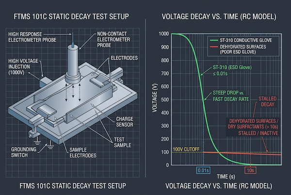
High-Voltage Corona Charging and Initial Potential Calibration: A standard test rig secures glove cut specimens to insulated test fixtures; A high-voltage power supply applies positive or negative DC static electricity of up to 5,000 volts or 1,000 volts to the test sample’s surface via non-contact needle electrodes or parallel-plate electrodes, rapidly saturating the glove’s surface material with charge and establishing a uniform, stable initial static potential of 1,000 volts on the sample’s surface;
Instantaneous Grounding and High-Response Non-Contact Detection: After a stable potential is established, the instrument’s high-speed disconnect switch instantly cuts off the high-voltage charging circuit and simultaneously connects the sample electrode to the ground reference; a non-contact high-speed electrostatic field tester (electrometer probe) mounted directly above the sample begins to continuously record the curve of the residual electrostatic potential on the sample surface over time with microsecond-level time resolution;
Determination of the cutoff threshold from 1,000 volts to 100 volts: The FTMS 101C strictly defines the charge decay time (Decay Time) as: the absolute physical time elapsed from the moment of grounding until the electrostatic potential on the sample surface gradually drops from an initial 1,000 volts to 100 volts (i.e., when 90% of the charge has been discharged); In high-end cleanrooms and wafer-level process standards, this decay time must be consistently maintained within 0.01 seconds (10 milliseconds); in some extremely sensitive scenarios, it must even reach the 0.005-second range to ensure that, during the brief interval between task transitions, the potential on the glove surface has completely returned to below the absolute safety threshold.
RC Circuit Modeling and Exponential Voltage Decay
Based on an analysis of electromagnetic fields and circuit equivalent models, the hand of a person wearing a glove, together with the chip pins being handled and the work surface, essentially forms a typical lumped-parameter first-order RC discharge circuit:
Series topology of the system’s equivalent capacitance and equivalent impedance: In this physical circuit, the dielectric constant and effective geometric thickness of the glove fibers and the rubberized coating determine the equivalent capacitance (C) at the contact interface, while the vertical volume resistance penetrating the glove’s thickness and the lateral leakage resistance at the glove’s surface together constitute the equivalent discharge resistance (R);
The Physical Nature of Exponential Voltage Decay: When a system charged with an initial voltage is grounded through the glove, the residual transient voltage in the circuit follows the classic exponential decay law: the residual voltage equals the initial voltage multiplied by the natural constant raised to the power of negative time divided by the time constant (RC); the system’s charge dissipation rate is determined solely by the circuit’s time constant (Tau = R × C); The smaller the time constant, the faster the charge dissipates;
Mathematical basis for a decay time of less than 0.01 seconds: In actual cleanroom assembly conditions, the parasitic capacitance at the interface is typically in the range of tens to hundreds of picofarads; If a static potential of 1,000 volts is to be rapidly attenuated to less than 100 volts within 10 milliseconds, calculations based on the exponential equation show that the total resistance of the glove’s equivalent discharge path must be strictly limited to between 10^7 and 10^8 ohms; If the glove’s overall impedance rises to 10^10 ohms or higher due to the use of low-quality chemical surfactants or a break in the conductive network, the circuit’s time constant will increase dramatically to several seconds or even tens of seconds. As a result, the glove will effectively lose its ability to dynamically dissipate charge on a high-speed assembly line, forcing operators to directly handle exposed wafers while carrying a high residual potential.
Suppressing Localized Charge Islands in Continuous Handling
Under high-speed production cycles, if the glove material lacks three-dimensional isotropic conductivity throughout its entire volume, highly destructive “localized charge islands” are likely to form on the microscopic surface:
Dead zones for charge capture caused by discontinuous conductive networks: Some low-end anti-static gloves have an excessively low proportion of conductive fibers during weaving, or feature a striped arrangement of conductive threads with overly wide spacing (greater than 10 millimeters); In microscopic areas of polyester or pure PU coating lacking conductive fiber coverage, electron migration paths are severely physically blocked; after contact and separation occur when grasping a material tray, the static charge accumulated in these tiny areas cannot rapidly migrate laterally into the main conductive lines, thereby forming independent charge islands on the fingertip surface—each with a diameter of only a few millimeters and a potential as high as several thousand volts;
Induction of secondary electric fields and induced discharges during workstation movement: Although the glove’s overall macroscopic average impedance may pass a simple two-point inspection, these locally trapped microscopic high-voltage charge islands act like miniature capacitors embedded in the fingertips; When the fingertips of a glove containing these charge islands hover over the surface of a sensitive integrated circuit, they excite strong localized mirror charges and non-uniform induced electric fields on the chip pins, directly causing near-field electric field-induced breakdown without physical contact;
The Suppression Effect of a Three-Dimensional Continuous Embedded Conductive Matrix: Truly compliant microelectronics-grade ESD gloves (such as those with micron-scale composite carbon fiber yarns precisely blended into the fabric base layer) construct a conductive percolation network in microscopic three-dimensional space, featuring node densities with spacings of less than 3 millimeters; Once a microscopic contact generates free charges due to friction or separation, the densely interwoven carbon fiber network immediately acts like a distributed drainage system, homogenizing and dispersing the localized excess charge along three-dimensional pathways within microseconds and guiding it to the ground terminal. This fundamentally eliminates any localized potential spikes and completely prevents the secondary induction threat posed by charge islands to precision components.
Quantitative Metrology Matrix: Physics, Test Standards, and Material Thresholds
In the fields of microelectronics manufacturing and semiconductor packaging and testing, if material qualification engineers rely solely on verbal technical assurances from manufacturers or vague “anti-static” labels, they are highly likely to expose the entire cleanroom production line to unknown risks of electrical breakdown. To establish quantifiable and traceable physical evaluation benchmarks, the electrical parameters of various protective gloves must undergo comprehensive, multidimensional comparative analysis under rigorous laboratory testing standards. By quantitatively analyzing the response characteristics of different material systems under extreme conditions, it is possible to clearly define the physical boundaries of materials—from high-insulation failure to controlled dissipation.
Cross-Standard Physical Parameters Comparison Table
The table below systematically compares the actual physical performance of four common glove material systems in the industry in terms of core electrical metrics, environmental adaptability, and discharge safety, providing rigorous data support for engineering selection:
| Material Classification System | Surface Resistivity (ANSI/ESD STM11.11) | Vertical Resistance (EN 1149-2 / EN 16350) | Static Charge Decay Time (FTMS 101C, 1000 V to 100 V) | Stability at Extremely Low Humidity (25% RH, 48-hour pre-conditioning) | Nanosecond-scale transient peak discharge current | Production Line Electrical Short Circuits and EOS Risk Rating |
| Standard Insulated Gloves(Unmodified Pure Polyester/Nitrile/Standard PU) | Greater than 1.0 x 10^12 ohms/cubic unit | Greater than 1.0 x 10^11 ohms | Greater than 60 seconds(Charge cannot dissipate spontaneously) | Very Poor(Maintains a highly insulated, charged state over the long term) | Zero(No spontaneous discharge, but induces strong field induction) | Extremely High(CDM breakdown induced by strong electric fields and particle adsorption) |
| Surfactant-Coated Gloves(Externally Sprayed Quaternary Ammonium Salt Anti-Static Agent) | 1.0 x 10^8 to 1.0 x 10^10 ohms/cubic unit(For humid environments only) | 1.0 x 10^9 to 1.0 x 10^11 ohms(Extremely unstable impedance) | 2.5 seconds to 15 seconds(Varies significantly with ambient humidity) | Complete Failure(Hydrated layer dries out, resistance skyrockets into the insulating range) | Low to moderate(Depends on the degree of localized drying of the surface layer) | Catastrophic(Root cause of batch-wide hidden breakdowns on production lines during the dry season) |
| Ultra-Pure Metal Conductive Gloves(All-Metal Wire / Ultra-High-Density Conductive Fabric) | Less than 1.0 x 10^5 ohms/cubic unit | Less than 1.0 x 10^5 ohms | Less than 0.001 seconds(Instantaneous avalanche-like discharge) | Very High(Unaffected by humidity) | Extremely intense(Can reach transient surges of several amperes) | Extremely High(Causes hard spark erosion and electric shock at live workstations) |
| Intrinsically Electrostatic Dissipative Gloves (ST-310)(13-Gauge Carbon Fiber/Polyester Blend + Conductive PU) | 1.0 × 10⁶ to 1.0 × 10⁸ ohms/cubic unit | 1.0 × 10⁶ to 1.0 × 10⁸ ohms(Fully compliant with EN 16350) | Less than 0.01 seconds(High-speed, controlled, gradual decay) | Very High(Intrinsic carbon black network, zero dependence on ambient humidity) | Strictly controlled(The impedance network spontaneously suppresses the peak current) | Absolutely Safe(Golden dissipation zone, also functions as a current-limiting safety valve) |
Interpreting the Metrology Divergence
A thorough analysis of the inflection points in the key physical parameters of the test matrix described above is crucial for correcting long-standing testing misconceptions within the procurement team:
The Disconnect Between Surface Resistance and Penetration Vertical Resistance: In actual testing, many quality control personnel often confuse two-dimensional surface resistance (measured in ohms or ohms/square) with three-dimensional penetration vertical resistance (measured in ohms). Surface resistivity is measured using concentric circular electrodes in accordance with ANSI/ESD STM11.11 and reflects the two-dimensional impedance of charge diffusion across the glove’s outer surface. Vertical resistance, on the other hand, is measured using cylindrical electrodes in accordance with EN 1149-2. This method forces the test current to penetrate vertically from the glove’s outer layer through the bottom of the liner into the metal base, reflecting the glove’s actual ability to dissipate charge safely to ground via the wearer’s body and the antistatic wrist strap;
Longitudinal insulation barriers masked by one-sided surface compliance: For low-quality gloves manufactured using surface spraying processes, or products where the surface coating is physically isolated from the inner knitted layer, the two-dimensional surface may yield a compliant dissipation impedance, but a high-insulation barrier layer with a resistance as high as 10^11 ohms may exist in the longitudinal thickness direction; Under such conditions, even if workers properly wear a grounded wrist strap, the charge on the glove’s surface remains firmly trapped by the insulating lining and cannot be conducted into the human grounding circuit, ultimately resulting in intense lateral discharge when the fingertips come into contact with a microchip;
Test Inflection Points and Intrinsic Conductivity Thresholds in Low-Humidity Environments: The most critical failure inflection point in the data tables occurs during pre-conditioned humidity testing at 25% RH; in low-humidity environments, the impedance of chemically coated gloves deteriorates precipitously, with static charge decay times extending uncontrollably from a few seconds to over tens of seconds—directly causing them to miss the millisecond-level operation cycles required for SMT placement and wafer handling;
Technical Lock-in of the Bidirectional Safety Window: The core advantage of intrinsically dissipative equipment, as exemplified by the ST-310, lies in strictly synchronizing two-dimensional surface resistivity with three-dimensional vertical resistance within the range of 1.0 × 10^6 to 1.0 × 10^8 ohms; This range perfectly avoids the risks of micro-crater damage and electric shock caused by transient high currents when the resistivity falls below 1.0 × 10⁵ ohms, while physically compressing the charge decay half-life to less than 0.01 seconds, ensuring zero-dead-zone, zero-delay charge dissipation protection under all cleanroom production conditions.
Engineering the Dissipative Asset: ST-310 13-Gauge Technical Profile
To completely eliminate the risk of electrostatic discharge in demanding microelectronics assembly and cleanroom operations, the development of protective equipment must go beyond merely compiling conceptual metrics; it must be grounded in the physical integration of materials science and micro-textile engineering. As an electrostatic protection asset tailored for high-density SMT production lines and microelectronics processing, the ST-310 achieves a physical integration of mechanical abrasion resistance and millisecond-level charge dissipation pathways within a 13-gauge medium-weight knitted structure through molecular-level topological restructuring of micron-scale conductive filaments and polymer coating .
Continuous Carbon-Polyester Knitted Core Mechanics
The fiber knitting process of the glove liner directly determines the integrity of its three-dimensional conductive pathways and its resistance to mechanical stretching :
13-gauge high-strength, low-dust polyester filament matrix: ST-310 employs a 13-gauge seamless knitting process, utilizing high-polymerization-degree, continuous polyester filaments as the structural framework; compared to conventional short-fiber spinning, these high-strength filaments are less prone to fiber pilling and particle shedding under high-frequency bending and repeated stretching at workstations, thereby eliminating the source of dust generation at the foundation;
Precision Blending of Composite Bicomponent Carbon Fiber Filaments: During the weaving process, micron-scale organic conductive bicomponent carbon fiber filaments are tightly wrapped and twisted around polyester filaments under constant tension, forming a three-dimensional continuous conductive grid network along the glove’s warp and weft directions with spacing strictly controlled within 3 millimeters; Carbon black particles are not merely coated onto the fiber surface but are permanently encapsulated and fused into the polymer filament core; even under high-frequency stretching and deformation at the finger joints, the microscopic interlocking nodes between the conductive filaments maintain physical contact;
Establishment of an isotropic current-dissipation network: This dense blended topological structure ensures that the glove exhibits highly consistent electrical conductivity in all directions; when triboelectric charges are generated on the palm or fingertips, the charges no longer remain trapped on localized surfaces but are instead conducted vertically through the thickness of the glove along the three-dimensional carbon fiber network within microseconds, forming an unobstructed three-dimensional dissipation pathway.
Full-Palm Micro-Dispersed PU Coating Grounding
In high-load workstations—such as heavy machinery assembly, handling live electrical fixtures, and transporting anti-static containers—gloves require not only fingertip sensitivity but also large-area, controlled discharge pathways:
A micro-dispersed system for full-palm conductive dip-coating formulations: Unlike conventional insulating PU dip-coating, the ST-310 full-palm polyurethane coating incorporates micron-sized, coupling-modified conductive carbon black fillers during the emulsion synthesis stage; Through high-speed shearing and ultrasonic homogenization dispersion technology, the carbon black particles form dense and uniform conductive microchannels within the polymer polyurethane matrix, eliminating insulating dead zones within the polymer;
Creating an extremely large closed-loop physical grounding contact area: The full-palm continuous coating provides the palm and palm center regions with a vast effective conductive grounding surface ; When assembly workers handle heavy-load conductive tote boxes, lift aluminum alloy jigs, or press their palms flat against a grounded anti-static mat, the large-area dipped coating forms a current-dissipating interface with ultra-low contact resistance the moment contact is made, allowing charges on the human body and materials to be smoothly conducted into the grounding circuit at a very high flux;
Engineered synergy of mechanical abrasion resistance and anti-slip grip: The microporous, breathable PU coating not only provides reliable micro-ohm-level dissipative impedance, but its unique micro-rough surface also gives the glove an extremely high coefficient of friction against both dry and wet surfaces; when gripping smooth metal trays, copper-clad laminates, or glass substrates, it effectively eliminates the risk of secondary electrostatic charging caused by micro-friction from slippage.
Washing Resilience vs. Chemical Surface Bleaching
The fundamental distinction between traditional chemically-coated anti-static gloves and intrinsically conductive gloves lies in the patterns of electrical resistance degradation when subjected to industrial cleaning and repeated use:
The “instant failure” trap of chemically-coated gloves during washing: Gloves that rely on externally sprayed or soaked quaternary ammonium salt surfactants have an anti-static coating bonded to the base fibers solely through weak physical adsorption; During cleaning with deionized water to cleanroom standards or in industrial washing cycles, water flow and mechanical agitation cause the surface chemical surfactants to rapidly dissolve and wash away; after just one routine wash and dry cycle, the surface resistance often experiences a precipitous rise, causing the gloves to degrade into complete insulators with a resistance greater than 1.0 × 10^11 ohms;
Zero-Drift Cleaning Characteristics of Physically Embedded Carbon Networks: The ST-310’s electrical conductivity stems entirely from the carbon nanonetwork cured within the fiber core and the uniformly dispersed carbon black crystals throughout the resin matrix; even after dozens of industrial cleaning, centrifugal dehydration, and clean drying cycles using an 18-megohm ultrapure water system, its microscopic carbon conductive network retains its lattice integrity, and no effective conductive material is ever leached out due to water-phase flushing;
High Convergence of Impedance Throughout the Entire Lifecycle: After multiple standardized industrial cleaning and aging tests, the ST-310’s vertical penetration resistance and surface resistivity remain firmly locked within the optimal electrostatic dissipation range of 1.0 × 10⁶ to 1.0 × 10⁸ ohms, eliminating the quality risk of glove impedance drift caused by washing and aging, and establishing a truly reliable ESD material defense barrier for enterprises throughout the entire product lifecycle.
Surface Resistivity vs. Vertical Resistance: Laboratory Testing Protocols
When establishing ESD quality acceptance criteria for microelectronics cleanrooms, many laboratory technicians often confuse “surface resistivity” with “vertical resistance,” or even hastily issue reports based on a single test fixture. In fact, there are fundamental differences in electromagnetic field distribution between the lateral discharge kinetics on a material’s surface and the three-dimensional vertical conduction mechanism that penetrates the thickness of a glove. Failure to clearly define the boundaries between these two laboratory testing methods makes it highly likely that gloves with critical defects will be overlooked during incoming quality control (IQC) inspections. To systematically understand the underlying interplay between these two testing systems at the standards level, as well as the technical guidelines of European and American standards, we recommend consulting our comprehensive pre-compliance analysis guide: en-16350-ansi-esd-antistatic-gloves-compliance.
2D Surface Resistivity via Concentric Ring Probes
According to the North American Electrostatic Discharge Association standard ANSI/ESD STM11.11, the core of measuring surface resistivity lies in capturing the confined diffusion behavior of charge on a two-dimensional plane:
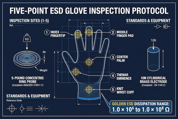
Mechanical loading with a 5-pound standard concentric ring probe: This standard specifies the use of a high-precision concentric ring electrode assembly with a self-weight of 5 pounds (approximately 2.27 kilograms); A conductive rubber pad with specific hardness and extremely low contact resistance is affixed to the base of the electrode. Through constant vertical gravitational force, it applies pressure to the glove specimen laid flat on a highly insulated test bench pad, ensuring complete contact between the electrode and the specimen surface and eliminating microscopic contact air gaps;
Two-dimensional lateral electric field vectors induced by the annular gap: The concentric probe consists of a central cylindrical electrode and an outer annular electrode arranged coaxially and concentrically; when the high-resistance meter applies a test voltage between the inner and outer electrodes, the electric field lines are forced to propagate within the annular gap between the outer edge of the inner electrode and the inner edge of the outer electrode; The current flows entirely in a two-dimensional lateral direction along the outer coating of the glove without penetrating the glove’s underlying layer;
Geometric Factor Conversion of Resistivity: Since the geometric dimensions of the inner and outer electrodes are precisely machined and strictly standardized, the surface resistance value directly read by the instrument can be accurately converted to the material’s two-dimensional surface resistivity in “ohms per square” using a fixed concentric circle geometric scaling factor (typically a constant of 10). This quantifies the resistance limit for the lateral dissipation of charge within the plane of the glove coating.
3D Through-Plane Vertical Resistance via EN 1149-2
Compared to the North American testing approach, which emphasizes surface diffusion, the European anti-static standard for protective clothing, EN 1149-2, and the specific standard for microelectronics gloves, EN 16350, focus their evaluation on the more practical three-dimensional vertical conductive path to ground:
A penetration circuit formed by a 10-newton cylindrical brass electrode and a metal base: In the EN 1149-2 test rig, the outer surface of the glove is laid flat face-down and in close contact with a grounded, mirror-polished stainless steel substrate; A cylindrical brass electrode with a base diameter of 25 millimeters is vertically pressed against the glove’s inner liner from above, applying a constant normal mechanical load of 10 newtons;
Three-dimensional impedance characterization of forced longitudinal penetration current: A DC voltage is applied directly between the upper cylindrical electrode and the lower metal base; electric field lines penetrate the glove specimen perpendicularly, passing through the inner lining to the outer coating; This path forces the current to travel the entire physical thickness of the “inner liner fiber network—dipped bonding interface—outer conductive coating,” accurately measuring the vertical resistance in absolute units of “ohms”;
Complete replication of human discharge in real-world work scenarios: The vertical resistance measured under EN 1149-2 directly reflects the actual physical conditions at the workstation—after an operator’s palms become sweaty, the sweat microclimate comes into contact with the glove lining, and the friction-generated charge must smoothly penetrate the glove’s thickness in the longitudinal direction and be conducted to ground via a grounded antistatic mat, a metal nozzle fixture, or a wrist strap; If a glove is only conductive horizontally on the surface while the inner lining is insulating in the vertical direction, such a pseudo-anti-static product will be immediately exposed under the EN 1149-2 columnar electrode test.
Voltage Switching Dynamics: 10V vs. 100V Open-Circuit Calibration
In field testing and laboratory calibration of high-resistance megohmmeters, the selection of the open-circuit test voltage directly determines the accuracy of impedance readings and is a key technical measure for preventing data falsification by suppliers:
Nonlinear conduction artifacts caused by material voltage dependence: The conductive behavior of polymers and microscopic composite materials does not strictly follow ideal Ohm’s law but exhibits significant voltage dependence; under high electric field strengths, microscopic insulating media that are normally non-conductive may undergo field-emission or transient localized dielectric breakdown, thereby producing false low-resistance readings on test instruments;
Automatic threshold switching between 10-volt and 100-volt test voltages: Rigorous ESD measurement procedures (such as ANSI/ESD STM11.11 and the IEC 61340 series) explicitly stipulate a stepwise voltage calibration logic:
When the measured resistance of the test specimen is 1.0 × 10⁶ ohms or less, the instrument must be strictly set to measure at the low open-circuit voltage of 10 volts to prevent overcurrent and device breakdown at low voltages;
When the resistance value is greater than or equal to 1.0 × 10⁶ ohms, the instrument is permitted to automatically or manually switch to a 100-volt open-circuit test voltage to detect weak currents in the high-impedance range;
Eliminate false compliance data caused by high-voltage breakdown: Many substandard glove manufacturers violate regulations during factory quality inspections by using excessively high open-circuit voltages—such as 250 volts or even 500 volts—throughout the testing process; the excessively high electric field forces its way through microscopic cracks in the glove’s insulating coating, artificially generating falsified “impedance-compliant” readings; Once these gloves are put into production, under actual SMT operating conditions involving low voltages of tens of volts, the insulating medium cannot be broken down, and the charge becomes completely trapped on the glove’s surface. Therefore, incoming inspection must strictly adhere to the standard graded switching procedures of 10 volts and 100 volts to resolutely eliminate loopholes that lead to false readings.
Failure Mode Mitigation: Nanoscale Gate Protection in High-Speed SMT
In modern high-density surface-mount technology (SMT) and advanced semiconductor packaging production lines, the fault-tolerance window for electrostatic control has been reduced to the micrometer and nanometer scales. Many manufacturing facilities encounter unrecoverable rework rates during Final Functional Testing (FCT), the root cause of which is often not equipment leakage or transient lightning strikes, but rather the failure of gloves worn by operators to intercept microcharges at the nanosecond level during manual intervention in feeding, placement verification, or housing assembly. To completely eliminate irreversible device damage, process engineers must draw upon the physics of solid-state microelectronics failure to systematically build a protective framework against ultra-micro electrical stress and combined mechanical damage.
Preventing Latent SiO₂ Gate Rupture in Advanced ICs
In nanoscale advanced processes and power semiconductor devices, the core structures of metal-oxide-semiconductor field-effect transistors (MOSFETs) and complementary metal-oxide-semiconductor (CMOS) devices are extremely fragile:
The breakdown voltage threshold of nanoscale gate dielectric layers: As chip process nodes shrink, the thickness of the silicon dioxide (SiO₂) dielectric layer—which isolates the gate from the channel within a MOSFET—has typically been reduced to less than a few nanometers; At the quantum mechanical scale, even a weak electrostatic potential of just 30 to 50 volts applied to the gate terminal can cause the local electric field strength across the nanoscale dielectric layer to instantly exceed the physical insulation breakdown limit of 10 meV/cm;
Microscopic Causes of Avalanche Multiplication and Microcraters: When weak static electricity accumulated on a technician’s hands is injected into the gate via the lead, the strong electric field triggers violent collision ionization and electron avalanche multiplication; The accompanying high-speed localized current density generates extreme Joule heating within nanoseconds, causing the originally dense and insulating silicon dioxide lattice to melt through instantly, forming nanoscale micro-melt pits, pinholes, or electromigration bridges formed by metal atoms;
The Deadly Trap of Latent Failures (“Walking Wounded”): Damage caused by these low-energy electrostatic pulses often does not result in an immediate and complete short circuit, but rather creates internal stress defects and high-leakage pathways within the semiconductor; Damaged chips may barely pass routine functional tests during final factory inspection; however, as the equipment remains powered on for extended periods at the end-user’s site and thermal stress accumulates over time, the damaged micro-melt pits continue to expand. This ultimately leads to catastrophic logic deadlocks or sudden system failures after several months of use, resulting in incalculable losses from recalls and compensation claims for the brand.
SMT Tape-and-Reel Peeling and Rapid Grounding
During loading, changeovers, and manual rework of defective components on high-speed SMT production lines, the frequency of dynamic high-voltage electrostatic discharges far exceeds that in static assembly environments:
High-density electrostatic discharges during tape peeling: Surface-mount components are commonly packaged in plastic tape-and-reel cassettes with a protective film. When an operator rapidly peels off the protective film or removes components from the reel cavity, the violent contact and rapid separation of the polymer films can instantly generate transient electrostatic potentials ranging from 3,000 to 8,000 volts at the peeling interface;
Induced Charge Capture During Pick-and-Place Operations: When a mechanical pick-and-place nozzle deviates and requires manual calibration, or when an operator’s fingers approach an exposed tape-and-reel, residual charges from the peeling process are rapidly induced onto the chip’s metal electrodes and lead frames. If there are dead zones in the insulation resistance of the operator’s gloves at this moment, the charges cannot dissipate within the microsecond window before contact;
Real-time transient clamping via a three-dimensional continuous dissipation network: Intrinsically dissipative gloves with a millisecond-level charge half-life can, within a few microseconds of the fingertip contacting the carrier tape or component lead frame, smoothly divert the dynamic charge generated by the separation process to the grounding system via an embedded continuous conductive network; This is equivalent to establishing an adaptive low-pass shunt channel around sensitive pins, neutralizing the charge before it has time to create a high potential difference across the gate dielectric layer.
Secondary Mechanical Protection in Mixed Electronics Handling
In real-world electronics manufacturing environments, workstations are often not limited to the assembly of single chips but instead face complex conditions where “mechanical sharp-edge operations” and “hypersensitive electrostatic control” intersect:
Coating delamination caused by sharp edges on sheet metal and PCB board edges: In the assembly of industrial control enclosures, server rack cabling, and the panel-cutting of large-size copper-clad laminates, the sharp edges of untreated cold-rolled steel stampings, aluminum alloy extrusions, and fiberglass board edges act like microscopic blades. The rubberized coating on standard anti-static gloves is extremely fragile; once scraped by metal burrs, the surface coating is highly prone to localized delamination, cracking, and peeling, exposing the inner insulating base fabric directly;
Mechanical damage poses a risk of localized insulation breakdown: Physical wear and fiber cuts on the glove’s surface directly sever the physical continuity of microscopic conductive pathways; when damaged areas come into contact with components, they lose their ability to dissipate static charge and instead become highly insulating friction points that generate static electricity, rendering the originally controlled anti-static barrier ineffective;
Cross-Category Mechanical and Electrostatic Composite Protection Solutions: For demanding mixed-use scenarios requiring the handling of precision integrated circuits while withstanding severe physical cuts and scratches, companies must move beyond the limitations of single-layer, lightweight gloves and adopt advanced composite equipment that integrates ultra-high-molecular-weight polyethylene (UHMWPE) or aramid cut-resistant fibers with an intrinsically conductive network; For systematic industrial solutions on how to withstand mechanical burrs from metal sheets and extend the wear resistance of front-line operations, please refer to our specialized cut-resistant engineering guide: Cut Resistant Work Gloves.
Technical & Compliance FAQ: Electrostatic Kinetics in Cleanroom Gloves
During routine audits of microelectronics manufacturing and semiconductor packaging and testing production lines, Quality Engineering (QE) and Electrostatic Discharge (ESD) managers often encounter technical disputes regarding discrepancies between laboratory data and on-site measurements. Addressing confusion over material units of measurement, safety boundaries for charged workstations, dynamic interference from ambient humidity, and disagreements over the selection of different coating structures, the following summarizes four of the most representative core technical issues and their physical explanations.
Why does surface resistivity (Ohms/sq) differ conceptually from resistance (Ohms)?
In industrial test reports, “surface resistance” (measured in ohms) and “surface resistivity” (measured in ohms per square) are often mistakenly used interchangeably, yet they have distinctly different physical definitions in electromagnetism:
Geometric Dependence of Resistance: Surface resistance measures the absolute impedance flowing across the sample surface between two contact electrodes under a specific electrode fixture configuration; this value is directly influenced by the sample test distance, electrode contact area, and geometric shape, and is considered an extrinsic physical quantity;
Geometric independence of surface resistivity: Surface resistivity is an intrinsic parameter characterizing the conductive properties of a material’s surface layer; it represents the resistance between two opposite sides of a square area on the material’s surface. Whether the side length of this square is 1 millimeter or 1 meter, as long as the current flows uniformly and parallel to the surface, the measured resistance value remains theoretically constant;
Mathematical Conversion of the Geometric Factor: When testing with concentric-circle probes in accordance with the ANSI/ESD STM11.11 standard, the raw impedance reading from the instrument is expressed solely as a resistance value; This impedance must be multiplied by a dimensionless geometric factor derived from the gap between the inner and outer electrodes of the concentric circle (typically, the probe constant conversion factor is approximately 10) to obtain the standard surface resistivity in “ohms per square”; therefore, when comparing material specifications, it is essential to clearly identify whether the measured parameter is absolute resistance or resistivity to avoid making erroneous acceptance decisions due to a difference of one order of magnitude.
Can a glove with a static decay time of less than 0.01 seconds cause an electric shock at live testing stations?
Many electrical safety supervisors are concerned: Does a glove with a static charge decay time of less than 0.01 seconds (i.e., extremely rapid charge dissipation) indicate that its internal conductivity is too high, which could cause workers to suffer an electric shock when they come into contact with live equipment? The answer is no, as long as the glove strictly falls within the electrostatic dissipative range (1.0 × 10⁶ to 1.0 × 10⁹ ohms):
Physical differences between high-voltage microcharges and low-voltage power-frequency sources: A decay time of less than 0.01 seconds is a discharge kinetics requirement for micro-static charges in the microampere range (such as a 1,000-volt static potential with a charge in the pico-coulomb range); it relies on the rapid redistribution of the electric field by a highly sensitive conductive micro-network, rather than requiring a zero-ohm short circuit;
Ohm’s Law Constraints for Series Current-Limiting Safety Valves: A lower limit impedance value of 1.0 × 10⁶ ohms (1 megohm) or higher forms an impenetrable series safety current-limiting resistor between the human body and the external circuit; According to Ohm’s Law, even if an operator accidentally comes into contact with a live test bench (such as 24 V, 48 V, or even 220 V AC test points), the leakage current flowing through the gloves and into the human body from the external operating voltage is physically limited to the microampere range (typically well below 1 milliampere);
Absolute intrinsic safety below the human perception threshold: This microampere-level leakage current is far below the human electric shock perception threshold (typically 1 milliampere) and the ventricular fibrillation danger threshold (tens of milliamps). It not only completely eliminates the destructive sparks generated by nanosecond-level hard discharges but also eliminates the risk of electric shock and muscle spasms for operators, establishing a perfect balance between device protection and personal safety.
How does relative humidity (RH) dynamically alter the RC time constant of cleanroom gloves?
Fluctuations in ambient air humidity can cause significant physical disturbances to the electrical discharge circuit of antistatic gloves. Essentially, this occurs by altering key parameters in the equivalent RC discharge model:
The effect of air humidity on the equivalent interfacial capacitance (C): Water molecules have an extremely high dielectric constant (approximately 80 at room temperature); when ambient relative humidity rises, the number of water molecules adsorbed on the surface of the polymer material increases, causing the local dielectric constant at the interface between the glove and the workpiece to increase, which in turn results in a slight rise in the system’s equivalent capacitance C;
Avalanche-like amplification of the equivalent resistance (R) in chemically coated gloves: The most dramatic effect is observed in the equivalent resistance R; for surface-coated chemical gloves, when relative humidity drops abruptly from 50% RH to 25% RH, the hydrated ionic conductive layer on the material’s surface completely dries out and breaks down, causing the overall resistance R to surge exponentially out of control by several thousand times (shooting directly from 10^8 ohms to over 10^11 ohms);
Discharge failure caused by a surge in the time constant τ: According to the RC discharge model, the time constant τ (where τ equals R multiplied by C) is amplified hundreds or even thousands of times due to the dramatic surge in resistance R; The charge decay, which would normally take only a few milliseconds, is forcibly extended to several seconds or even tens of seconds, causing the gloves to completely lose their ability to dynamically dissipate charge under the rapid production line cycle; this is also why the international standard EN 16350 and incoming inspection procedures in high-end manufacturing facilities strictly require that glove samples undergo 48 hours of pre-conditioning in an extremely dry environment (25% RH) before testing.
Why does the finger-dipped ST-300 exhibit different surface dissipation behavior than the palm-coated ST-310?
As part of the same intrinsic carbon fiber-blended conductive glove system, the finger-dipped ST-300 and the full-palm-coated ST-310 demonstrate distinct functional and physical divisions in their charge dissipation kinetics under actual working conditions:
Differences in how microclimate sweat regulation affects the dynamic impedance of the inner lining: The palm of the fingertip-dipped ST-300 features a fully breathable, uncoated fabric structure, allowing trace amounts of sweat vapor from the palm to evaporate and escape rapidly. The microenvironment inside the glove lining is less prone to the accumulation of conductive salts, and the longitudinal volume resistivity is highly dependent on the microscopic contact between the composite carbon filaments in the fiber matrix, making it suitable for wafer handling with tweezers and microscopy workstations that require ultra-high dexterity and low particle release;
Advantages of the ST-310’s Full-Palm Coating with Large-Area Closed-Loop Ground Contact: The ST-310, with its full palm coated in conductive PU, features micron-sized conductive carbon black fillers uniformly dispersed within the coating layer; When operators handle SMT trays, grip metal fixtures, or support conductive transport boxes with both hands, the ST-310 can establish a high-density closed-loop contact area with ground spanning hundreds of square centimeters within microseconds; its comprehensive surface discharge flux far exceeds that of finger-dipped gloves, which rely solely on localized fingertip contact;
Precise balance between mechanical workload at workstations and slip-resistant grip: The full-palm coating provides a more uniform and stable impedance distribution, more effectively preventing the accumulation of non-uniform localized charges caused by palm friction. It is particularly suitable for high-speed SMT front-end work areas that require frequent handling of heavy-duty jigs, insertion and removal of large connectors, and have higher demands for abrasion and scratch resistance.
Enterprise QA & Procurement Protocol: Validating Static Dissipation at the Source (CTA)
In the fields of high-precision microelectronics manufacturing and semiconductor packaging and testing, the final line of defense against the risk of electrostatic discharge (ESD) is not post-incident failure analysis (FA), but rather rigorous quality control at the source (IQC) and strict procurement standards. The primary reason low-cost chemically treated foam gloves have managed to slip through the cracks in some factories is that certain quality control teams lack standardized on-site re-inspection procedures, often blindly approving them based solely on a static test report provided by the supplier. To completely eliminate this systemic quality risk, a company’s Quality Engineering (QE) and supply chain procurement departments must establish standardized incoming material sampling inspection and direct-sourcing mechanisms based on physical impedance verification.
In-House Incoming QA Verification Protocol
For anti-static gloves arriving in bulk, corporate quality assurance departments must abandon subjective sensory inspections and strictly enforce the following standardized “5-Point High-Resistance Meter Incoming Inspection Protocol”:
Controlled-environment pre-humidification and batch sampling (AQL sampling threshold): In accordance with ISO 2859-1 (GB/T 2828.1), the normal inspection single-sampling plan (typically set at General Inspection Level II, AQL 0.65), to randomly select samples from the incoming batch; before testing, place the sampled gloves in a controlled constant-temperature and constant-humidity chamber and allow them to acclimate for at least 24 hours under harsh, low-humidity conditions (23 degrees Celsius, 25% RH) to eliminate false compensation of the gloves’ microscopic resistance caused by moisture in the ambient air;
Test Bench Insulation and Ground Loop Calibration: Testing must be conducted on an antistatic insulated test bench with a surface insulation resistance greater than 1.0 × 10¹² ohms; connect the grounding terminal of a high-precision megohmmeter to a standard ground, and perform zero-point and open-circuit drift calibration using a high-resistance standard calibration block before taking official readings;
Two-dimensional pressure application using concentric ring probes and cylindrical electrodes: Use a 5-pound concentric ring double-weight probe compliant with the ANSI/ESD STM11.11 standard to measure the two-dimensional surface resistivity of the glove’s palm coating, and a 10-newton cylindrical brass electrode compliant with the EN 1149-2 standard to measure the glove’s vertical resistance to longitudinal penetration; The use of handheld, simple two-point testers for rough testing is strictly prohibited;
Automatic stepwise verification of open-circuit test voltage: Strictly lock the test voltage switching logic of the high-resistance meter—when the impedance reading is less than 1.0 × 10⁶ ohms, force the instrument to record the reading at a test voltage of 10 volts; When the reading reaches 1.0 × 10⁶ ohms or higher, the instrument must switch to the standard 100-volt test voltage; the use of 250-volt or 500-volt ultra-high-voltage testing is strictly prohibited to resolutely prevent false compliance loopholes caused by high-voltage breakdown of the insulating medium;
Five-Point Dispersion and Decay Assessment: Precisely select five representative physical points on a single glove—“index finger tip, middle finger pad, center of the palm, lateral side of the thenar eminence, and the ribbed cuff at the wrist”—and read data sequentially; The resistance values at all measurement points for the entire batch must consistently fall within the optimal dissipation range of 1.0 × 10⁶ to 1.0 × 10⁸ ohms; If the resistance at any single point exceeds 1.0 × 10⁹ ohms or falls below 1.0 × 10⁵ ohms, the batch is immediately deemed non-compliant with electrostatic physical uniformity requirements, and the entire batch must be rejected and isolated for return.
Deploying Certified Dissipative Assets on Sensitive Production Lines
For multinational electronics manufacturing services (EMS) providers engaged in large-scale mass production, as well as wafer fabrication cleanrooms and automotive electronics assembly lines, the use of non-standard personal protective equipment (PPE) or PPE sourced through multiple layers of distributors directly drives up the hidden total cost of ownership (TCO) for the entire production line. Only by working directly with source manufacturers that possess end-to-end R&D and weaving capabilities can a traceable, auditable protective barrier be established from the ground up:
Direct Assurance from the Source Factory and Batch COA Traceability: SQG relies on its own modern textile and polymer dipping production facilities to implement closed-loop, industrial-scale quality control across the entire supply chain—from the blending of conductive two-component carbon fiber filaments and fully automated seamless knitting to the homogenized emulsification of micron-level conductive polyurethane (PU) formulations; Every batch of products shipped from the factory is accompanied by a formal Certificate of Analysis (COA) detailing ambient temperature and humidity, test electrode parameters, and vertical/surface dual impedance curves, ensuring that every box of gloves is backed by comprehensive physical anti-static data;
We support bulk procurement and customized agreement lock-ins: To meet the large-scale supply chain procurement needs of international EMS giants, we have established a standardized minimum order quantity (MOQ) mass production system and global logistics delivery channels. We can provide stable long-term production scheduling and supply chain inventory guarantees in accordance with customers’ stringent cleanroom particle release standards and anti-static resistance tolerances;
Request an Original Manufacturer’s Engineering Verification Sample Kit (Master Sample Kit): To assist semiconductor engineers and ESD committees in comprehensively re-testing the charge decay half-life and continuous wear life of gloves under harsh, dry, low-humidity conditions, SQG is now opening an official sample channel to technical and procurement teams from companies that have passed our qualification review. You can immediately submit your operating condition requirements to our application engineering experts and request a factory-sealed engineering sample kit: Request Enterprise ESD Sourcing Consultation & Master Sample Kit.


